Memory Interface IP for TSMC
Welcome to the ultimate Memory Interface IP for TSMC hub! Explore our vast directory of Memory Interface IP for TSMC
All offers in
Memory Interface IP
for TSMC
Filter
Compare
532
Memory Interface IP
for TSMC
from 18 vendors
(1
-
10)
-
TSMC CLN4P 4nm DDR5 PHY - 6400Mbps
- Supports DDR5
- DFI 5.1 compliant
- Supports x4, x8 and x16 DRAMs
- Up to 72 bits wide and up to 4 ranks
-
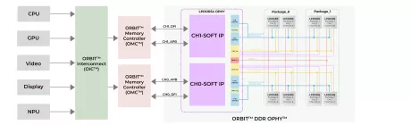
LPDDR5X DDR Memory Controller
- JEDEC LPDDR5X/LPDDR5 devices compatible
- Data rates up to 8533Mbps
- Multiple ARM AMBA AXI4/AHB/APB & Custom interfaces
-
ONFI 4.1 NAND Flash Controller & PHY & IO Pads on 16nm
- Page Size – 2KB, 4KB, 8KB, 16KB
- Bank/chip select options
- Programmable timing
-
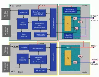
MIPI M-PHY G4 Designed For TSMC 28nm HPC+
- Compliant to MIPI Alliance Standard for M-PHY specification Version 4.1
- Supports M-PHY Type-I system
- Support for Clock and Data Recovery Options
-
ONFI 4.1 NAND Flash Controller & PHY & IO Pads on 28nm
- Page Size – 2KB, 4KB, 8KB, 16KB
- Bank/chip select options
- Programmable timing

-
ONFI 4.1 NAND Flash Controller & PHY & IO Pads on 12nm
- Page Size – 2KB, 4KB, 8KB, 16KB
- Bank/chip select options

-
GDDR6 PHY IP for 12nm
- JEDEC JESD250 compliant GDDR6 support
- X16 mode, X8 mode, and pseudo-channel mode
- Low frequency RDQS mode support
-
GDDR6 PHY
- Single configuration supports one GDDR6 device per channel (coplanar) or two GDDR6 devices per channel (clamshell)
- DFI PHY Independent Mode for initialization and training
- Adaptive and continuous timing recovery
- Internal and external datapath loop-back modes
- Transmit crosstalk cancelation of immediate neighbors
- Per-bit DFE, CTLE, and FFE equalization
-
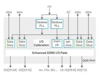
DDR5/4 PHY for TSMC 7nm
- Application optimized configurations for fast time to delivery and lower risk
- Memory controller interface complies with DFI standards up to 5.0
- Internal and external datapath loop-back modes
- Per-bit deskew on read and write datapath
-
DDR/LPDDR PHY
- DDR5/4/3 training with write-leveling and data-eye training
- Optional clock gating available for low-power control
- Internal and external datapath loop-back modes
- I/O pads with impedance calibration logic and data retention capability
- Programmable per-bit (PVT compensated) deskew on read and write datapaths
- RX and TX equalization for heavily loaded systems