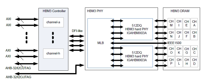
IGAHBMX03A is a HBM3 (High Bandwidth Memory) PHY IP compliant to the JEDEC HBM3 DRAM Specification Rev 0.95. Built on TSMC 7nm process node, it supports data rate up to 7200 Mbps per data pin with DFI 1:4 clock frequency ratio (controller clock : WCK = 1:4). Signal and power integrities were analyzed with GUC design flow to ensure all signal and power requirements could be met.
TSMC CLN7FF HBM3 PHY
Overview
Key Features
- HBM3 data rate up to 7200 Mbps
- Supports DFI-like 1:4 clock frequency ratio (controller clock : WCK = 1:4)
- Supports only BL8
- Supports AWORD/DWORD bus parity
- Supports programmable parity latency, PL=0 and 2 of DQ parity function
- Supports HBM3 data bus inversion (DBI)
- Supports 64DQ ECC/SEV per channel
- HBM3 hard PHY delivered as a hard macro which includes I/O, PLL, and DLL
- Supports internal loopback and READ/WRITE BIST
- Supports HBM3 loopback test, includes MISR and LFSR mode
- Supports IEEE 1500 instruction
- Supports HBM3 lane repairs with redundant pin for row/column/data
- Supports HBM3 duty cycle adjuster (DCA ) and duty cycle monitor (DCM)
Block Diagram
Technical Specifications
Foundry, Node
TSMC 7nm CLN7FF
TSMC
Silicon Proven:
5nm