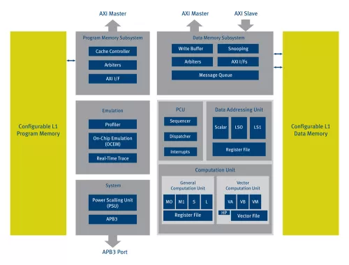
The fifth generation of the widely licensed Ceva-XC architecture, the Ceva-XC323 is optimized for IoT communication applications as well as UE terminals. The Ceva-XC323 delivers highly powerful vector capabilities alongside a general computation engine to supply the performance and flexibility demanded by various IoT communication applications.
Highly powerful and scalable multi-mode communication processor for IoT wireless applications
Overview
Key Features
- Fully programmable DSP processor architecture: Two vector processing units - each unit operates on 256-bit vector registers offering a powerful SIMD engine
- Up to 8 simultaneous instructions (8-Way VLIW)
- Efficient DSP support for non-vectorized data
- Efficient support for control and ANSI-C operations
- Extremely powerful computation capabilities
- 32 16x16-bit MAC operations
- 64 arithmetic operations per cycle
- Over 200 16-bit operations in a cycle
- Exceptional power efficiency
- Incorporates Power Scaling Unit – PSU 2.0
- Dedicated power optimized Tightly Coupled Extensions (TCE)
- Enhanced power-optimized pipeline
- Scalable and configurable architecture for use in a wide range of wireless communication applications and devices through different processors, configurations and optional modules
- Scalable computation capabilities and memories
- Configurable utilization of optional instruction sets
- Uniquely designed for communication applications
- High flexibility SIMD programming model with intra-vector permutation capabilities
- Optimized modem instruction sets including high precision ISA, ML MIMO detectors, filtering, complex data permutations, and more
- Tightly Coupled Extensions (TCE)
- A selection of coprocessor units allowing efficient low power implementation of demanding transceiver algorithms including:
- MLD MIMO detector up to Rank4
- 3G De-spreader units
- Fast Hadamard Transform
- DFT
- FFT
- Viterbi decoding
- LLR processing and HARQ combining
- User-defined coprocessor interface enabling customers to reuse their existing proprietary IP
- Offers parallel computing in parallel to the DSP functions
- Offloading the core and lowering its frequency to minimize power consumption
- A selection of coprocessor units allowing efficient low power implementation of demanding transceiver algorithms including:
- Complete memory subsystem
- Includes tightly coupled memories (TCM), caches, AXI system interfaces, APB interface, advanced DMA controller,, message queues, emulation and profiling modules.
- Ensures easy integration and optimal performance in Target SoCs
- Integrates an innovative second generation Power Scaling Unit (PSU 2.0) offering significant energy savings for both battery-operated and stationary devices
- Advanced power management for both dynamic and leakage power
- Multiple voltage domains associated with the functional units
- Multiple operational modes ranging from full operation, to debug bypass, to memory retention, to complete power shut-off (PSO)
Block Diagram

Technical Specifications
Maturity
In Production
Availability
Available
Related IPs
- Multi-protocol wireless platform integrating Bluetooth Dual Mode, IEEE 802.15.4 (for Thread, Zigbee and Matter)
- 8-stage superscalar processor that supports ISO 26262 ASIL (Automotive Safety Integrity Level) -D level functional safety for automotive applications
- Scalable and flexible display processor
- Scalable Ultra-High Throughput Lossy and Lossless JPEG 2000 Encoder
- Highly Scalable and Efficient Second-Generation ML Inference Processor
- Scalable Edge NPU IP for Generative AI