HBM2E/HBM2 Controller

Overview

Highest performance IP for graphics, AI/ML

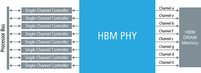
The High-Bandwidth Memory generation 2/2E PHY (HBM2E/2 PHY) is silicon-proven and is available in four process nodes: PHYs, achieving breakthrough performance, low energy per bit, and low area relative to the data bandwidth. It is engineered to quickly and easily integrate into SoCs and is verified as part of a complete memory subsystem solution. The HBM2E/2 PHY IP is an ideal solution for artificial intelligence (AI), high-performance computing (HPC), and image processing applications.

Key Features

  • High-performance command queue placement and command execution selection
  • Optimized throughput of unique pseudo-channel interleaving
  • Lowest latency for data-intensive applications
  • Low-power control and advanced low-power modes with power-down and self-refresh
  • Memory controller interface is based on DFI 5.0
  • DFI frequency ratio of 2:1
  • Memory BIST feature

Benefits

  • Proven: Silicon characterization reports available
  • Low Latency: For data-intensive applications
  • High Performance: Highest performance HBM2E at 3.6Gbps. Interposer optimized for best signal integrity.
  • Low Power and Area: Low power control: advanced low power modes

Block Diagram

HBM2E/HBM2 Controller Block Diagram

Technical Specifications

Samsung
Pre-Silicon: 10nm
×
Semiconductor IP