Flash Controller IP
Welcome to the ultimate Flash Controller IP hub! Explore our vast directory of Flash Controller IP
All offers in
Flash Controller IP
Filter
Compare
22
Flash Controller IP
from 13 vendors
(1
-
10)
-
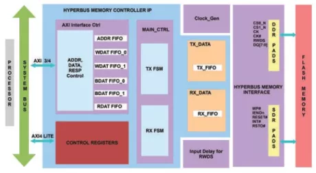
Hyperbus Flash Memory Controller
- Compatible with spansion hyperbus based memory products.
- 0 Wait State Write Burst Operation for HyperBus memory on AXI interface of up to 256 words.
-
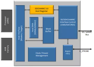
SD 3.0 / SDIO 3.0 / eMMC 5.0 Host Controller
- Memory Card / Form Factors:
- IP Details:
-
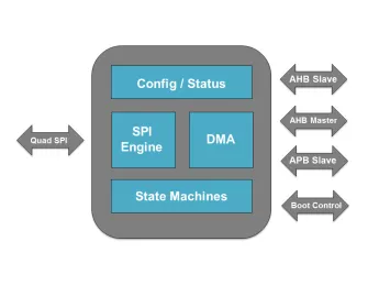
Quad-SPI FLASH Controller AHB
- AHB Memory Mapped Access
- Auto-Copy DMA Boot Support
- DMA controller
-
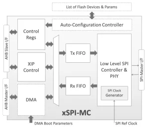
xSPI Flash Memory Controller
- Compatible to most SPI protocols used by the NOR-Flash vendors including xSPI (JEDEC’s JESD251), and Xccela
- Single, Dual, Quad, Twin-Quad and Octal SPI lanes. Single and Dual Transfer Rate (STR and DTR)
- Programmable bit-length and number of SPI lanes used for command, address, latency (dummy cycle) and data. Programmable command encoding
- XIP - Allows AHB bus masters to read directly from the flash with zero software overhead.
-
ONFI 3.2 NAND Flash Controller
- Compliant to ONFI revision 3.2 standard
- Supports NV-DDR2 mode of operation supporting up to 200MHz
- Supports NV-DDR mode of operation supporting up to 100MHz
- Supports legacy Asynchronous devices operating from 10MHz to 50MHz
-
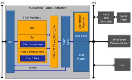
SD 3.0 / SDIO 3.0 Combo Device Controller
- Meets SD Memory Card Physical Layer Specification version 3.0
- Meets SDIO card specification ver 3.0
- Host clock rate variable between 0 and 208 MHz
- All SD bus modes supported including SPI, 1 and 4 bit SD.
-
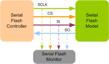
Serial Flash Verification IP
- Follows Serial Flash specification as defined in WINBOND, MICRONIC, MACRONIX, MICRON, SPANSION, Silicon Storage technology (SST) and many more.
- Supports software and hardware Reset
- Supports quad peripheral interface (QPI) reduces instruction overhead
- Supports allows true XIP (execute in place) operation
-
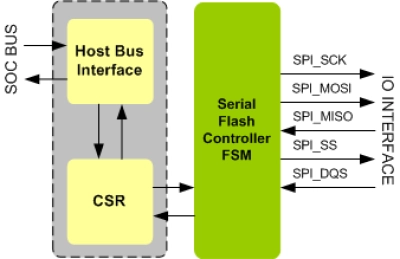
Serial Flash Controller IIP
- Compliant with Flash Devices from major Flash Device Vendors.
- Full Flash with SPI Master Functionality.
- Supports 3 modes of operation
- Slave Mode - Accessing flash device through CSR registers from SOC Slave interface
-
PCIe-NVMe SSD Controller Platform
- Compliant to NVMe specification (pass UNH-IOL compliance test)
-
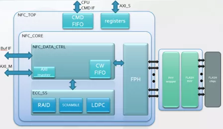
NAND Flash Controller (NFC) IP for SSD Controller
- Support all kinds of 2D/3D, SLC/MLC/TLC/QLC NAND Flash
- Supports 8KB~32KB NAND page size
- Support 1 to 8 FLASH channels
- Support all Flash command & optional command