Compression IP for SMIC
Welcome to the ultimate Compression IP for SMIC hub! Explore our vast directory of Compression IP for SMIC
All offers in
Compression IP
for SMIC
Filter
Compare
8
Compression IP
for SMIC
from 4 vendors
(1
-
8)
-
LVDS interfaces
- Wide operating range
- High data rates
- Very flexible programmability
- Excellent signal integrity
- TIA/EIA644A LVDS and sub-LVDS compatibility
- Receiver also compatible with LVPECL

-
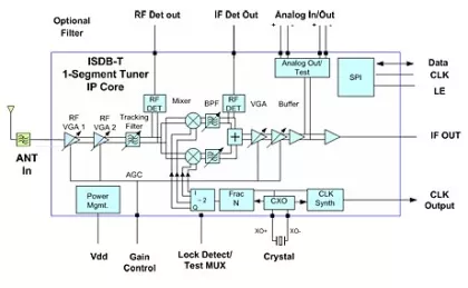
ISDB-T1, Segment Tuner (470-860MHz UHF)
- High Performance
- Configurable 3/4 wire controller
- Self calibrating and programmable filter corner frequencies
- 8 Bit electronically tunable tracking filter

-
Camera sub-LVDS/mini-LVDS/LVDS/HiSPi(SLVS-400, HiVCM)/MIPI-DPHY/CMOS 6-7mode Combo-Receiver 1.5Gbps
- MIPI DPHY v1-1/MIPI CSI/TIA/EIA-644 LVDS/SLVS-400 compliant
-
FPD-link, 30Bits Color LVDS Receiver, 150Mhz (SVGA/WXGA)
- 1P6M layout structure based on 0.18um 1P6M 1.8V generic logic process.
- 3.3V/1.8V 10% supply voltage, 0/+125C
- Complies with OpenLDI specification for digital display interfaces and LVDS IEEE Standard 1596.3-1996+ ANSI/TIA/EIA-644-A Specifications.
- Up to 3.15Gbps bandwidth (8 to 90Mhz pixel clock for 1 channel)
-
Triple HD-video AFE digitizer - 10bits/170Mhz - 8bits/205Mhz
- Triple channel video 10bits digitizer 170Mhz
- 0.5 to 1V analog input range
- 3.3V/1.8V ±10% supply voltage, -40/+125°C
- 1P6M layout structure based on 0.18um 1P6M 3.3V/1.8V generic logic process.
-
Triple DAC 10-Bits, voltage output - 10Mhz, 3.3V/1.3V full-scale
- Programmable full scale : 3V or 1V.
- 10 Bits resolution.
- 10MS/s update rate.
- Adjustable max output current 24, 30 or 36mA.
-
Triple Video DAC 10-Bits, 240Mhz
- 10-Bits Resolution
- 240MS/s Update Rate
- 3.3V ±10% supply voltage, -40/+125°C temperature.
- 1P6M layout structure based on 0.18um 1P6M 3.3V/1.8V generic logic process.
-
Audio PLL - Fractional-N ±0.05 ppm accuracy
- Fractional-N PLL : ± 0.05 ppm accuracy
- Eliminates VCXO/DCXO requirements
- 10-40 Mhz input
- Audio clock supports 256*fs & 384*fs