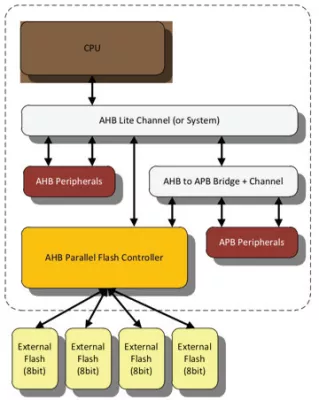
The AHB Parallel Flash Controller allows an AHB Master (usually a CPU) to read, program, or erase the connected arrangement of external parallel SuperFlash devices. The controller implements a set of configuration registers on an APB interface, while Flash accesses occur via an AHB interface. It also implements several modes of operation to facilitate these functions. During normal operation, AHB reads are translated into Flash reads by the controller directly. So, the controller functions as an AHB to Flash Bus Bridge in these instances. Other supported functions, such as Flash program and erase require some software involvement.
The AHB Parallel Flash Controller supports wide range of clock frequencies, timing values for the various Flash transfers can be configured via the APB registers.
AHB Parallel Flash Controller
Overview
Key Features
- Interfaces AHB bus to Parallel SuperFlash device(s)
- AMBA® AHB Compatible
- Supports 8-bit, 16-bit and 32-bit external modes
- Supports word (32-bit) AHB accesses to all configurations
- Supports byte (8-bit) and halfword (16-bit) AHB accesses to some configurations
- Programmable timing configurations for different Flash transactions
- Programmable regions for write protection
Block Diagram
Deliverables
- Verilog Source
- Complete Test Environment
- AHB Bus Functional Model
- C-Sample Code
Technical Specifications
Maturity
Silicon Proven
Availability
Now