Vendor:
Veriest Solutions Ltd.
Category:
SPI / QSPI XSPI
Quad-SPI FLASH Controller AHB
The Veriest Serial Flash Controller Design IP offers a rich set of features to facilitate easy access to Serial Flash devices.
Overview
The Veriest Serial Flash Controller Design IP offers a rich set of features to facilitate easy access to Serial Flash devices. The CPU can boot directly from the Serial Flash through the memory emulation interface. Alternatively the Serial Flash controller can copy a code image from the serial Flash device to CPU instruction memory prior to CPU boot. The Serial Flash Controller has an internal DMA controller which can be configured to copy code from the serial flash device to any target destination in the system. The Serial Flash Controller is compatible with advanced Flash devices supporting Quad-SPI and Execute-in-Place (XIP) as well as legacy devices using serial SPI. There are also useful features such as Device Detection, Serial Flash Integrity check using CRC-32 Serial FLASH image write and Device Direct Access to gain access to all the internal register set of the serial flash device.
Key features
- AHB Memory Mapped Access
- Auto-Copy DMA Boot Support
- DMA controller
- Flash Device Direct Access
- Serial Flash Device Detect
- Built-In-Self-Test (BIST)
- SPI Serial Mode
- SPI Quad Mode
- Bit Banging
- 3 / 4 Byte Addressing
- XIP Execute-In-Place
- AHB Slave Interface
- AHB Master Interface
- APB Slave Interface
- Boot Control Interface
- Interrupt
- Configuration and Status Registers
- SFLASH Image Write
- SPI clock rate configurable
Block Diagram
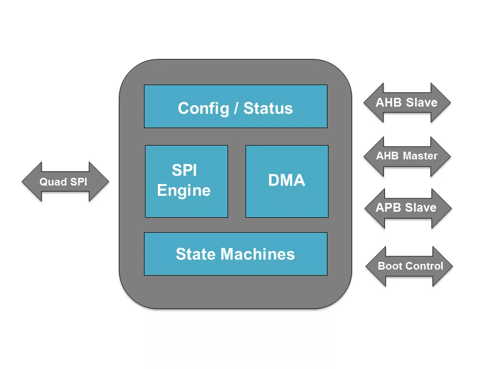
VV1200 block diagram
Benefits
- Low Gate Count
- Low Power Consumption
- Fully Verified in with Advanced Function Verification
- Spyglass Lint Validated
- Standards Compliant
- Silicon Proven Core
Applications
- General System on Chip Use
What’s Included?
- Synthesizable Verilog RTL
- Verilog test bench and test cases
- System Verilog verification environment and test cases
- Detailed block diagram and technical documents
Specifications
Identity
Part Number
VV1200
Vendor
Veriest Solutions Ltd.
Type
Silicon IP
Provider

Veriest Solutions Ltd.
HQ:
Israel
Veriest is an international design house providing forefront ASIC and FPGA design and verification services, as well as cutting edge EDA verification tools and platforms.
Veriest's portfolio of clients includes the full range of globally established industry leaders, defense companies, and also startups at preliminary stages of developing high-end chip technology.
Veriest was founded in 2007 by VLSI experts credited with rooted knowledge and experience in the field of ASIC and FPGA design.
Veriest is headquartered in Bnei Brak, Israel with R&D also in Belgrade, Serbia. Its team of 70 engineers constitutes the key players in projects at the forefront of chip technology.
We have made it our mission to provide our customers with complete quality solutions suited to the various phases of a product's life cycle.
Our skilled and creative team can effectively promote architecture design, implementation, system integration and advanced verification.
We are committed to answering industry demands relying on our wide range of field-proven methodologies and industry know-how, devising the working model that ideally accommodates the customer's needs.
Learn more about SPI / QSPI XSPI IP core
Unleashing the Power of Communication: Exploring the XSPI Protocol and Arasan Chip Systems' XSPI IP Portfolio
Frequently asked questions about SPI / QSPI / xSPI IP cores
What is Quad-SPI FLASH Controller AHB?
Quad-SPI FLASH Controller AHB is a SPI / QSPI XSPI IP core from Veriest Solutions Ltd. listed on Semi IP Hub.
How should engineers evaluate this SPI / QSPI XSPI?
Engineers should review the overview, key features, supported foundries and nodes, maturity, deliverables, and provider information before shortlisting this SPI / QSPI XSPI IP.
Can this semiconductor IP be compared with similar products?
Yes. Buyers can compare this product with similar semiconductor IP cores or IP families based on category, provider, process options, and structured technical specifications.