USB 3.0 PHY - GF 28SLP18 x1 OTG, East/West poly orientation

Overview

The USB-C 3.0 and USB 3.0 PHY IP provide designers with the industry's best combination of low area and low power with support for the leading process technologies from 65-nm to 14/16-nm FinFET. Both the USB-C and USB 3.0 PHYs offer a single efficient GDSII design that supports all four USB 3.0 speed modes (SuperSpeed, High-Speed, Full-Speed, and Low-Speed). To maximize battery life in mobile applications, the USB-C/USB 3.0 PHYs are designed to minimize power consumption and standby current. In addition, the USB-C 3.0 femtoPHY is optimized to support the USB Type-C connectivity specification.

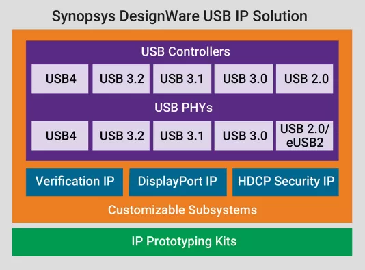
The USB IP is the most certified USB IP solution in the industry. With over 3,000 design wins and approximately three billion silicon-proven units shipped, the vendor complete USB IP solution, consisting of digital controllers, PHYs, verification IP, IP Prototyping Kits and IP software development kits, enables designers to lower integration risk and speed time-to-market.
Key Features

  • Part of a comprehensive IP solution including xHCI host and device controllers, PHYs, verification IP, IP Prototyping Kits and IP software development kits
  • Designed for advanced 1.8V CMOS planar bulk and FinFET process nodes
  • USB-C femtoPHY IP supports USB Type-C specification
  • USB-C/USB 3.0 femtoPHY on 14/16-nm FinFET and 28-nm processes offers 50% smaller area use, high performance, and advanced power features
  • Integrated PHY includes transmitter, receiver, PLL, digital core, and ESD
  • Design minimizes area and power
  • High yield: Designed to improve key operating margins by having less sensitivity to variations due to foundry process, chip and board parasitics, and process device variations
  • The USB 3.0 PHY IP is USB-IF Certified

Block Diagram

USB 3.0 PHY - GF 28SLP18 x1 OTG, East/West poly orientation Block Diagram

Technical Specifications

×
Semiconductor IP