CCIX 1.1 Controller
Overview
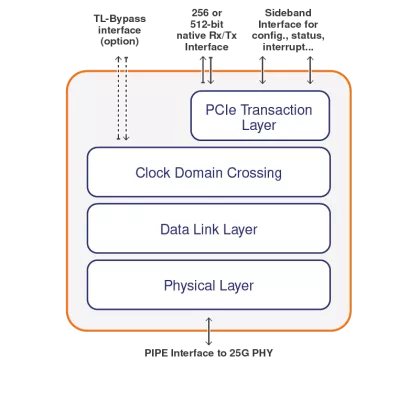
Rambus CCIX 1.1 Controller is a configurable and scalable PCIe controller Soft IP designed for ASIC and FPGA implementation. The XpressCCIX Controller IP supports the PCI Express 5.0, 4.0 and 3.1/3.0 specifications, as well as with version 4.x and 5.x of the PHY Interface for PCI Express (PIPE) specification, and supports the CCIX Extended Speed Mode as defined in the CCIX Base Specification 1.0. The IP can be configured to support endpoint, root port, switch port, and dual-mode topologies, allowing for a variety of use models. The provided Graphical User Interface (GUI) Wizard allows designers to tailor the IP to their exact requirements, by enabling, disabling, and adjusting a vast array of parameters, including CCIX ESM mode, data path size, PIPE interface width, low power support, SR-IOV, ECC, AER, etc. for optimal throughput, latency, size and power. XpressCCIX IP is verified using multiple PCIe VIPs and testsuites, and integrated with select CCIX 20G/25G compatible PHYs. XpressCCIX Controller IP for PCIe 5.0 with CCIX ESM support is the #1 choice for designers requiring enterprise-class features, highest performance, reliability, and scalability.
Key Features
- PCI EXPRESS
- Supports the PCI Express 5.0, 4.0, 3.1/3.0, and PIPE 4.x (8-, 16-, 32- and 64-bit) specifications
- Compliant with PCI-SIG Single-Root I/O Virtualization (SR-IOV) Specification
- Supports Endpoint, Root-Port, Dual-mode, Switch port configurations
- Supports x16, x8, x4, x2, x1 at 32 GT/s, 16 GT/s, 8 GT/s, 5 GT/s, 2.5 GT/s speeds
- Supports AER, ECRC, ECC, MSI, MSI-X, Multi-function, P2P, crosslink, and other optional features
- Additional optional features include OBFF, TPH, ARI, LTR, IDO, L1 PM substates, etc.
- CCIX SUPPORT
- Implements DVSEC Capability
- Supports x16, x8, x4, x2, x1 at CCIX ESM data rate 1, 20 Gb/s or 25 GB/s
- USER LAYER INTERFACE
- 512-bit transmit/receive low-latency user interface for both PCIe and CCIX traffic
- User-selectable Transaction/Application Layer clock frequency
- Sideband signaling for PCIe configuration access, internal status monitoring debug and more
- Optional Transaction Layer bypass
Benefits
- Track record of silicon proven PCIe 5.0 designs guarantees first-time silicon success
- Target ASIC/SoC and FPGA interchangeably and seamlessly with same RTL code
- Robust solution verified using multiple 3rd -party Verification IP (VIP) and testsuites
- Freedom to choose from a variety of pre-integrated, pre-verified, silicon-proven PHY IP
- Dedicated IP customization, verification, and design integration team available to help with improvement
- Recognized first-class technical support ensures timely resolution of issues
Block Diagram
Applications
- HPC,
- Cloud Computing,
- AI,
- Machine Learning,
- Enterprise,
- Networking,
- Automotive,
- AR/VR,
- Test and Measurement
Deliverables
- Verilog RTL,
- Supporting Documentation
Technical Specifications
Foundry, Node
Any
Maturity
In production
Availability
Available