DDR5 PHY IP
Welcome to the ultimate DDR5 PHY IP hub! Explore our vast directory of DDR5 PHY IP
All offers in
DDR5 PHY IP
Filter
Compare
475
DDR5 PHY IP
from 18 vendors
(1
-
10)
-
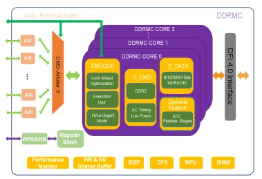
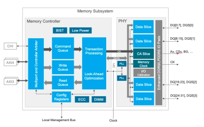
DDR5 IP solution
- Compatible with DDR5 up to 4800Mbps
- AXI compliant multi-ports, and data width, FIFO depth, command queue depth configurable
- DFI5.0/4.0 compliant interface between controller and PHY
- Support ECC (error correcting code)
-
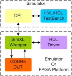
GDDR5 Synthesizable Transactor
- Supports 100% of GDDR5 protocol standard JESD212C
- Supports all the GDDR5 commands as per the specs
- Supports all types of timing and protocol violation detection
- Supports up to 8GB device density
-
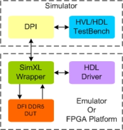
DDR5 DFI Synthesizable Transactor
- Compliant with DFI 5.0 Specification.
- DFI-DDR5 Applies to :
- DDR5 protocol standard JESD79-5 & JESD79-5 Rev1.40 (Draft) Specifications
- Supports all Interface Groups.
-
GDDR6 Memory Controller IP
- JEDEC GDDR6 standard JESD250B
- Fast frequency switching
- Flexible Configuration
-
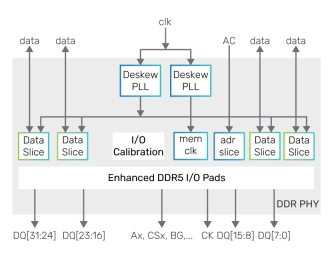
DDR PHY
- DDR5/4/3 training with write-leveling and data-eye training
- Optional clock gating available for low-power control
- Internal and external datapath loop-back modes
- I/O pads with impedance calibration logic and data retention capability
- Programmable per-bit (PVT compensated) deskew on read and write datapaths
- RX and TX equalization for heavily loaded systems
-
DDR5/4 PHY for TSMC 7nm
- Application optimized configurations for fast time to delivery and lower risk
- Memory controller interface complies with DFI standards up to 5.0
- Internal and external datapath loop-back modes
- Per-bit deskew on read and write datapath
-
DDR/LPDDR PHY
- DDR5/4/3 training with write-leveling and data-eye training
- Optional clock gating available for low-power control
- Internal and external datapath loop-back modes
- I/O pads with impedance calibration logic and data retention capability
- Programmable per-bit (PVT compensated) deskew on read and write datapaths
- RX and TX equalization for heavily loaded systems

-
DDR5/4 PHY - LRDIMM Add-On
- Supports JEDEC standard DDR5 and DDR4 SDRAMs
- High-performance DDR PHY supporting data rates up to 8400 Mbps
- PHY independent, firmware-based training using an embedded calibration processor
- Supports up to 4 trained states/ frequencies with <3μs switching time

-
DDR5/4 PHY V2 - TSMC N7
- Supports JEDEC standard DDR5 and DDR4 SDRAMs
- High-performance DDR PHY supporting data rates up to 8400 Mbps
- PHY independent, firmware-based training using an embedded calibration processor
- Supports up to 4 trained states/ frequencies with <3μs switching time

-
DDR5/4 PHY V2 - TSMC N6
- Supports JEDEC standard DDR5 and DDR4 SDRAMs
- High-performance DDR PHY supporting data rates up to 8400 Mbps
- PHY independent, firmware-based training using an embedded calibration processor
- Supports up to 4 trained states/ frequencies with <3μs switching time
