LPDDR5 IP for TSMC
Welcome to the ultimate LPDDR5 IP for TSMC hub! Explore our vast directory of LPDDR5 IP for TSMC
All offers in
LPDDR5 IP
for TSMC
Filter
Compare
11
LPDDR5 IP
for TSMC
from 5 vendors
(1
-
10)
Filter:
- 7nm
-
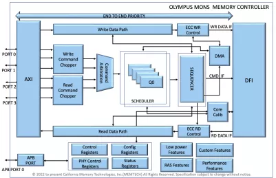
LPDDR5X DDR Memory Controller
- JEDEC LPDDR5X/LPDDR5 devices compatible
- Data rates up to 8533Mbps
- Multiple ARM AMBA AXI4/AHB/APB & Custom interfaces
-
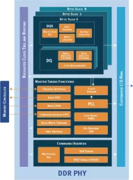
LPDDR5/4/4X PHY - TSMC N7 for Automotive, ASIL B Random, AEC-Q100 Grade 2
- Supports JEDEC standard LPDDR5X, LPDDR5, LPDDR4 and LPDDR4X SDRAMs
- Support for data rates up to 6400 Mbps
- Designed for rapid integration with Synopsys’ LPDDR5/4/4X controller for a complete DDR interface solution
- DFI 5.0 controller interface

-
LPDDR5/4/4X PHY - TSMC N7
- Supports JEDEC standard LPDDR5X, LPDDR5, LPDDR4 and LPDDR4X SDRAMs
- Support for data rates up to 6400 Mbps
- Designed for rapid integration with Synopsys’ LPDDR5/4/4X controller for a complete DDR interface solution
- DFI 5.0 controller interface

-
TSMC CLN7FFLVT 7nm LPDDR5 PHY - 6400Mbps
- Supports LPDDR5
- DFI 5.1 compliant
- Supports x4, x8 and x16 DRAMs
- Up to 72 bits wide and up to 4 ranks
-
TSMC CLN7FF 7nm LPDDR5 PHY - 6400Mbps
- Supports LPDDR5
- DFI 5.1 compliant
- Supports x4, x8 and x16 DRAMs

-
LPDDR5X Secondary/Slave (memory side!) PHY
- JEDEC standard LPDDR5X @ 8533Mbps (Mbits per second per pin)
- Flexible channel architecture – 16- or 32-bit data path widths, supporting either single x32 channel or two x16 channels – 64-bit support, supporting two x32 channels
- Support for byte-mode DRAM devices for high capacity systems
- ZQ Calibration
-
LPDDR5 Secondary/Slave (memory side!) PHY
- JEDEC standard LPDDR5 @ 6400 Mb per second per pin.
- Flexible channel architecture – 16- or 32-bit data path widths, supporting either single x32 channel or two x16 channels – 64-bit support, supporting two x32 channels
- Support for byte-mode DRAM devices for high capacity systems
- ZQ Calibration
-
LPDDR5/4/4X PHY in TSMC (N7) for Automotive
- Low latency, small area, low power
- Compatible with JEDEC standard LPDDR5 SDRAMs up to 6400 Mbps
- Compatible with JEDEC standard LPDDR4 and LPDDR4X SDRAMs up to 4267 Mbps
- DFI 5.0 compliant interface to the memory controller
-
LPDDR5/4/4X PHY in TSMC (16nm, 12nm, N7, N6, N5)
- Low latency, small area, low power
- Compatible with JEDEC standard LPDDR5 SDRAMs up to 6400 Mbps
- Compatible with JEDEC standard LPDDR4 and LPDDR4X SDRAMs up to 4267 Mbps
- DFI 5.0 compliant interface to the memory controller
-
LPDDR5/4X/4 Combo PHY & Controller
- LPDDR5 and LPDDR4/4X modes & signaling, rates from 20Mbps up to 6400Mbps (LPDDR5) and 4266Mbps (LPDDR4/4X), respectively
- x16/x32/x64 data path interface extendable
- 1.05V/1.1V JEDEC IO standard, support 1.05V and 1.1V LVSTL I/Os
- Support LPDDR4X 0.6V IO voltage and LPDDR5 0.5V/0.3V IO voltage