Memory Interface IP for TSMC
Welcome to the ultimate Memory Interface IP for TSMC hub! Explore our vast directory of Memory Interface IP for TSMC
All offers in
Memory Interface IP
for TSMC
Filter
Compare
45
Memory Interface IP
for TSMC
from 9 vendors
(1
-
10)
Filter:
- 7nm
-
LPDDR5X DDR Memory Controller
- JEDEC LPDDR5X/LPDDR5 devices compatible
- Data rates up to 8533Mbps
- Multiple ARM AMBA AXI4/AHB/APB & Custom interfaces
-
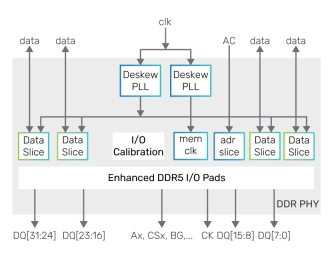
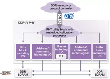
DDR5/4 PHY for TSMC 7nm
- Application optimized configurations for fast time to delivery and lower risk
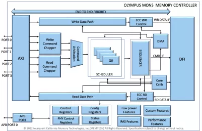
- Memory controller interface complies with DFI standards up to 5.0
- Internal and external datapath loop-back modes
- Per-bit deskew on read and write datapath
-
HBM2E PHY V2 - TSMC 7FF18
- Complete HBM2/HBM2E IP solution, including PHY, controller and verification IP, reduces integration risk while minimizing time-to-market
- 2.5D interposer expertise and reference designs
- Supports 2.5D-based JEDEC standard HBM2/HBM2E SDRAMs with data rates up to 3200 Mbps

-
HBM2E PHY V2 (Hard 1) - TSMC 7FF18
- Complete HBM2/HBM2E IP solution, including PHY, controller and verification IP, reduces integration risk while minimizing time-to-market
- 2.5D interposer expertise and reference designs
- Supports 2.5D-based JEDEC standard HBM2/HBM2E SDRAMs with data rates up to 3200 Mbps
-
LPDDR4X multiPHY - TSMC N7
- Supports JEDEC standard LPDDR4X, LPDDR4, LPDDR3, DDR4, DDR3, and DDR3L (1.35V DDR3) SDRAMs
- Support for data rates up to 4,267 Mbps (process dependent)
- Designed for rapid integration with Synopsys Enhanced Universal DDR Memory/Protocol Controllers (uMCTL2/uPCTL2) for a complete DDR interface solution
- PHY independent, firmware-based training using an embedded calibration processor

-
DDR4 PHY - TSMC N7
- Supports JEDEC standard DDR4, DDR3, and DDR3L SDRAMs
- High-performance DDR PHY supporting data rates up to 3200 Mbps
- Compatible with JEDEC compliant DDR3/4 UDIMMs and RDIMMs as well as DDR4 LRDIMMs
- Supports up to 16 logical ranks for high capacity memory requirements
-
LPDDR5/4/4X PHY - TSMC N7 for Automotive, ASIL B Random, AEC-Q100 Grade 2
- Supports JEDEC standard LPDDR5X, LPDDR5, LPDDR4 and LPDDR4X SDRAMs
- Support for data rates up to 6400 Mbps
- Designed for rapid integration with Synopsys’ LPDDR5/4/4X controller for a complete DDR interface solution
- DFI 5.0 controller interface

-
LPDDR5/4/4X PHY - TSMC N7
- Supports JEDEC standard LPDDR5X, LPDDR5, LPDDR4 and LPDDR4X SDRAMs
- Support for data rates up to 6400 Mbps
- Designed for rapid integration with Synopsys’ LPDDR5/4/4X controller for a complete DDR interface solution
- DFI 5.0 controller interface

-
DDR5/4 PHY V2 - TSMC N7
- Supports JEDEC standard DDR5 and DDR4 SDRAMs
- High-performance DDR PHY supporting data rates up to 8400 Mbps
- PHY independent, firmware-based training using an embedded calibration processor
- Supports up to 4 trained states/ frequencies with <3μs switching time

-
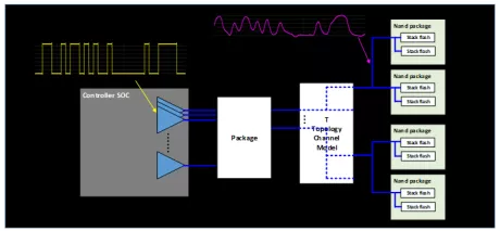
ONFI IO v5.1, 3.6GT/s, TSMC N7, 1.2V, N/S orientation, H&V cell
- Supports ONFI 6.0(4.8Gbps), ONFI 5.1(3.6Gbps), ONFI 5.0(2.4Gbps), ONFI 4.1(1.2Gbps), ONFI 4.0(800Mbps) & ONFI 3.2(533Mbps)
- Power-sequence free
- Provides multi-driving-strength selection
- Provides CTT mode and LTT mode