The SPI-MEM-CTRL core from Alma Technologies offers the interconnection between a host and an SPI Flash memory device. The SPI-MEM-CTRL supports Single, Dual Input, Dual Input/Output, Quad Output and Quad Input/Output SPI protocol accesses and optionally includes Boot and Execute On-The-Fly support.
The core automatically identifies a variety of serial flash memories and communicates with the attached device at the maximum possible bandwidth. Register accesses are used to insert access requests and read/write data into/out SPI-MEM-CTRL core. Communication with devices other than those automatically identified, is also feasible as the core can be programmed with the memory device parameters. The SPI-MEM-CTRL can read, write or erase any part of the memory.
The core is rigorously verified. A complete verification environment that helps designers verify the functionality and compliance of the core, and additional aids for system-level simulation are available.
Single, Dual and Quad SPI Flash Controller with Boot and Execute On-The-Fly Features
Overview
Key Features
- Device Independent
- Automatic identification of a variety of memories
- Configurable memory features to allow support of less standard Serial Flash devices
- Ability to communicate with up to 8 Serial Flash devices
- Supports memories with densities greater than 128Mbits
- Efficient Bandwidth Utilization
- Automatic identification of maximum bandwidth Extended SPI access mode among:
- single SPI
- dual output SPI
- dual input / output SPI
- quad output SPI
- quad input / output SPI
- Flexible Access Model
- Registered mapped I/O
- Host issues access request, reads and writes data via register accesses
- Read access size from 1 byte up to the entire memory size
- Read accesses starting from any address offset
- Write access sizes from 4 bytes up to the entire memory size
- Write accesses starting from any address offset that is multiple of 4
- Erasure of:
- any sector (4KB)
- any block (64KB)
- whole chip
- Ease of Integration
- Auto-detection of a wide set of Serial Flash devices to minimize programming overhead
- Auto-detection of the fastest way to read or program the memory, to maximize bandwidth and minimize programming overhead
- Deep Power-down Mode support to minimize power consumption
- Block Read Interface simplifies read transfers implementing a DMA mechanism.
- Block Read Interface can be enabled to automatically initiate a read transfer after powering-up.
- Design Quality
- Robust verification with integrated testbench environment.
- Scan-ready design
- Clear text VHDL or Verilog RTL source for ASIC designs, or pre-synthesized & verified Netlist for Altera, Lattice, Microsemi and Xilinx FPGA and SoC devices
- Release Notes, Design Specification and Integration Manual documents
- Bit Accurate Model (BAM) and test vector generation binaries, including sample scripts
- Self checking testbench environment, including sample BAM generated test cases
- Simulation and sample Synthesis (for ASICs) or Place & Route (for FPGAs) scripts
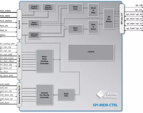
Block Diagram
Deliverables
Technical Specifications
Maturity
Silicon Proven
Availability
NOW
Related IPs
- SPI FLASH Controller with Execute in place – XIP (SINGLE, DUAL and QUAD SPI Bus Controller with DDR / DTR support and optional AES Encryption)
- Host controller IP for controlling flash and other devices on the SPI bus: Quad SPI, Octal SPI, and xSPI
- QSPI FLASH Controller – XIP functionality (SINGLE, DUAL and QUAD SPI Bus Controller with Double Data Rate support)
- Serial Peripheral Interface – Master/Slave with Octal, Quad, Dual and Single SPI Bus support
- Dual WideBand Frequency Synthesizer with Integrated VCO and Loop Filter - GlobalFoundries 55nm
- FSPI Controller – XIP functionality (SINGLE, DUAL, QUAD and OCTAL SPI Bus Controller with Double Data Rate support)