The Universal NAND Flash Controller (UNFC) IP core is designed specifically to enable commodity Flash memory to be effectively used in enterprise storage applications requiring high reliability and large interconnect bandwidth. Using the pre-validated UNFC IP allows greatly reduced time-to-market for storage OEMs desiring higher IOPS benefitting from lower cost SLC, MLC & TLC / QLC NandFlash memory.
The UNFC is full-featured, easy to use in Arria 10 FPGA designs with pre-integrated Aria PHY-Lite interface and an Avalon backend.
NAND flash Controller using Altera PHY Lite
Overview
Key Features
- ONFI 5.x Compliant
- SLC / MLC / TLC / QLC
- SDR modes 0 to 5
- NVDDR modes 0 to 5
- NVDDR-2 modes 0 to 8
- NVDDR-3 modes 0 to 10
- NV-LPDDR-4 modes 0 to 10
- Avalon interface
- Up to ECC 84-errors / 1k block
- Configurable Data block size
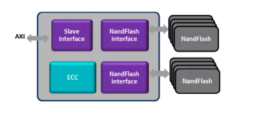
Block Diagram
Deliverables
- Verilog RTL source code
- Synthesis scripts
- Simulation testbench
- Technical documentation
- Technical support
Technical Specifications
Maturity
in production
Related IPs
- NAND Flash Controller
- NAND Flash Controller using Xilinx RX/TX Bit Slice
- NAND Flash controller supporting MLC Flash with multi-bit correction BCH ECC code
- Complete memory system supporting any combinations of SDR SDRAM, DDR, DDR2, Mobile SDR, FCRAM, Flash, EEPROM, SRAM and NAND Flash, all in one IP core
- AHB Compliant Nand Flash Controller
- NAND Flash controller for synchronous ONFI 2.1 NAND device, SLC/MLC support with BCH code