The L8051XC1 core implements an MCS®51-compatible microcontroller that is specially designed to match the timing and peripherals of legacy 8051 MCU based systems.
The core can be configured to execute an instruction every 12, 6, or 4 clock cycles. Architectural extensions are user-selectable, including multiple data-pointers, a multiply-division unit, and a power management unit. Furthermore, the 8051 CPU can be coupled with a wide range of peripherals matching the behavior and timing of peripherals found in legacy architectures from Intel, Phillips/NXP, Siemens/Infineon, Maxim/Dallas, Texas instruments and others. Several pre-configured versions are offered; custom variations are also available.
The L8051XC1 runs legacy code, but new software development is facilitated through CAST’s on-chip debugging option, and debug pods that cooperate with IAR Embedded Workbench & Keil uVision™ IDEs.
This new product builds on CAST’s experience with hundreds of 8051 IP customers going back to 1997. Designed for easy reuse in ASICs, structured ASICs, or FPGAs, the core is strictly synchronous, with positive-edge clocking (except in the optional debug & SPI modules), synchronous reset, and no internal tri-states. Representative 40nm ASIC results show the core to be conservative in its use of space, requiring just 7,000 to 40,000 gates.
Legacy-Configurable 8051-Compatible Microcontroller
Overview
Key Features
- Fully compatible with the MCS® 51 instruction set
- Configurable CPU architecture: 12, 6, or 4 clock cycles per machine cycle
- Extensive set of optional features and peripherals
- JTAG-based On-Chip Debug Support (OCDS)
- Integration with IAR Embedded Workbench & Keil uVision™ IDEs
- Options and Peripherals
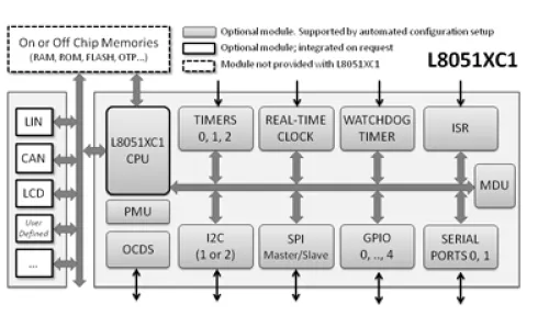
- A wide range of architectural options and peripherals is available for integration with the L8051XC1, and more peripherals can be developed on demand. The following is partial list of the off-the-shelf available peripherals:
- External Memory Interface:
- One, two or eight Data Pointers for fast data block transfer
- Additional Arithmetic Unit supports data pointers, auto-increment/-decrement, and auto-switch
- Supports external DMA controller through HOLD function
- Program memory write mode
- Direct Memory Access (DMA) Controller
- Multiplication-Division Unit
- 37 to 119 external Special Function Registers
- Interrupt Controller with two or four priority levels, and six or eighteen interrupt sources
- Up to five Parallel I/O Ports
- Serial 0 full-duplex serial interface (80C51-like), equipped with an additional baud rate generator
- Serial 1 (asynchronous-only version of Serial 0) interface
- SPI Master/Slave interface
- One or two I2C™ Master/Slave interfaces
- Timers 0, 1 and Timer 2 with Compare/Capture (80C515-like)
- 15-bit programmable Watchdog Timer
- Real Time Clock
- Power Management Unit with power-down modes (IDLE/STOP)
Block Diagram
Applications
- The L8051XC1 MCU core is especially effective for extending the lifetime of existing systems where an originally-used discrete 8051 chip is difficult to replace, or the designer wishes to consolidate a multi-board system into a single FPGA or ASIC.
Deliverables
- The core is available in ASIC (synthesizable HDL) or FPGA (netlist) forms, and includes everything required for successful implementation. ASIC versions include:
- HDL RTL source code
- Easy-to-use configuration tool (with configurable versions)
- An example chip implementation, which uses the core in a sample system
- Sophisticated self-checking HDL Testbench including everything needed to test the core (Verilog versions use Verilog 2001)
- Simulation script, vectors, and expected results
- Synthesis script
- Comprehensive user documentation, including detailed specifications and a system integration guide
Technical Specifications
Maturity
Production Proven
Availability
Now