Die to Die IP
Welcome to the ultimate Die to Die IP hub! Explore our vast directory of Die to Die IP.
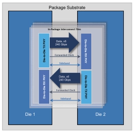
A die-to-die IP is a functional block that provides the data interface between two silicon dies that are assembled in the same package. Die-to-die interfaces take advantage of very short channels to connect two dies inside the package to achieve power efficiency and very high bandwidth efficiency, beyond what traditional chip-to-chip interfaces achieve.
All offers in
Die to Die IP
Filter
Compare
86
Die to Die IP
from 18 vendors
(1
-
10)
-
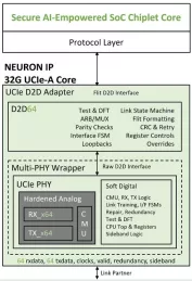
UCIe PHY & D2D Adapter
- 32Gbps UCIe-Advanced (UCIe-A) & Standard (UCIe-S)
- UCIe v1.1 specification
-
UCIe Die-to-Die Controller IP
- High Configurability and Customizability
- Comprehensive Verification
-
2-16Gbps Multi-Protocol IO Supporting BOW, OHBI and UCIe
- High Bandwidth Density and Data Rates
- Package Configurability
- Energy Efficiency
- Fully Integrated Solution
-
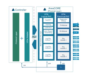
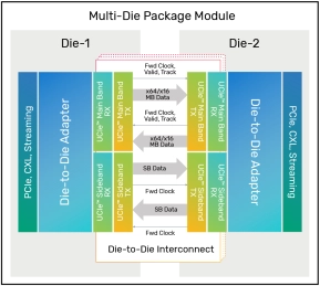
Universal Chiplet Interconnect Express (UCIe™) PHY
- Supports up to 32Gbps per pin including 4/8/12/16/24Gbps
- Forwarded clock, track, and valid pins
- Sideband messaging for link training and parameter exchange
- KGD (Known Good Die) testing capability
- Redundant lane repair (advanced)
- Width degradation (standard)
- Lane reversal

-
40G UltraLink D2D PHY
- Innovative mixed-signal architecture to achieve high bandwidth, ultra low latency and low power
- Flexible data rate from 20Gbps to 40Gbps
- Built-in self-test features to ensure “known good die”
- Interoperable between different technology nodes and foundries
- Easy routing and straightforward integration
- Achieves better than 10-15 bit error rate (BER) without requiring forward error correction (FEC)
- Integrated scrambling and lane de-skew functionality
- Supports -40ºC to 125ºC industrial temperature range
-
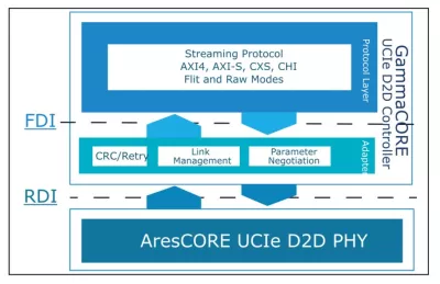
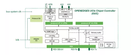
Universal Chiplet Interconnect Express (UCIe™) Controller
- Lowest latency controller for data intensive die-to-die applications
- Supports single and multiple PHY modules
- CXS, CHI C2C, AXI, PCIe, CXL, and streaming protocols
- CRC and retry mechanism
- Sideband messaging for link training, parameter exchange, and vendor defined messages
- Link State Management
- Parameter Negotiation
-
Ultralink Controller
- 1Tbps/mm unidirectional bandwidth
- Low power and low latency
- Easy routing and straightforward integration
-
UCIe Die-to-Die Chiplet Controller
- High configurability and customizability
- Defines packets to communicate with a link partner using different AXI parameters
- Supports raw streaming modes
- Provides various Flit formats in UCIe v1.1 (filt format 2: 68B flit format, flit format 3/4: standard 256B flit format, and flit format 5/6: latency optimized 256B flit format)
-
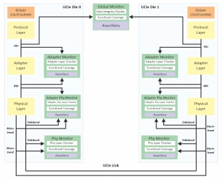
UCIe Verification IP
- Available in native SystemVerilog (UVM/OVM /VMM) and Verilog.
- Unique development methodology to ensure highest levels of quality.
- Availability of various Regression Test Suites.
- 24X5 customer support.
-
UCIe 2.0 Verification IP
- Available in native SystemVerilog (UVM/OVM /VMM) and Verilog.
- Unique development methodology to ensure highest levels of quality.
- Availability of various Regression Test Suites.
- 24X5 customer support.
