The V4 ColdFire Processor Core is a high-performance implementation of the ubiquitous ColdFire architecture from Freescale Semiconductor, offering over 500 DMIPS of performance. Fully code compatible with V1 and V2 ColdFire devices, the V4 ColdFire architecture offers high-end features such as cache and Memory Management Unit (MMU), plus advanced arithmetic units including hardware divider (DIV), enhanced MAC (EMAC), and an optional Floating Point Unit (FPU).
The V4 ColdFire Core is the same IP implemented in Freescale’s MCF5441x microcontrollers. By either including or excluding the FPU, you can configure the V4 ColdFire Core to match either the V4e or V4m processor configuration used in Freescale MCF54xx devices. And, like the V1 and V2 ColdFire cores, the V4 ColdFire Core benefits from the extensive ecosystem of development systems, tools, and software supporting the ColdFire architecture.
ColdFire V4 Processor
Overview
Key Features
- 32-bit address and data paths
- Variable-length RISC architecture for maximum code density
- ColdFire ISA Revision C plus dedicated instructions for integrated arithmetic hardware (DIV, EMAC, and FPU)
- Branch acceleration for minimal change-of-flow execution time
- Big-endian data organization
- Up to 64 KB of local RAM with single-cycle access
- Separate instruction/data caches (up to 32 KB each)
- MMU with variable page sizes (up to 16 MB)
- AMBA 2 AHB system bus with master and slave ports
- Master port for V4 ColdFire accesses
- Slave port for external AHB master access to V4 ColdFire local RAM
- Bootable from local RAM or system (AHB) memory
- STOP mode for low-power operation
- ColdFire Debug Architecture Revision D+
- Background Debug Mode (BDM)
- Real-Time Trace (RTT)
- Real-Time Debug (RTD)
- On-chip, 128-entry trace buffer for low-cost trace over BDM
- Fully synchronous, synthesizable, scannable design
Benefits
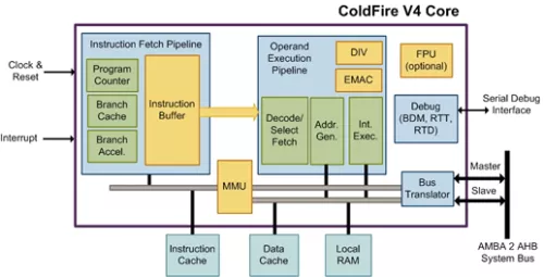
- The ColdFire V4 Core achieves best-in-class 32-bit processor performance through a combination of features including a 9-stage pipeline with limited superscalar (dual-issue) instruction execution. The 9-stage pipeline consists of a 4-stage Instruction Fetch Pipeline (IFP) and 5-stage Operand Execution Pipeline (OEP) decoupled by a FIFO instruction buffer. The optional FPU executes instructions in parallel with the OEP. Separate clocks for the CPU and system bus enable the V4 ColdFire Core to operate at a higher frequency than the rest of the system.
- The ColdFire V4 Core achieves 1.54 DMIPS/MHz and can run at up to 345 MHz in a 90-nm process technology.
- Local RAM and cache, running at the CPU clock rate, further maximize system efficiency by reducing the overall number of system bus accesses, leaving more system bus bandwidth available for other system resources such as other another processor or DMA controller. The system bus is the industry standard AMBA 2 AHB. The ColdFire V4 Core includes both an AHB master port and an AHB slave port, which enables an external AHB master to access the ColdFire V4 local RAM, either while the ColdFire V4 Core is running or while it is in low-power STOP mode
Block Diagram
Video
Putting the ColdFire Family to Work for You
Deliverables
- Synthesizable Verilog source code
- Integration testbench and tests
- Documentation
- Scripts for simulation and synthesis with commonly-used EDA tools
Technical Specifications
Maturity
Silicon Proven
Availability
Now