The 3.3V capable GPIO is an IP macro for on-chip integration. It is a 3.3V general purpose I/O built with a stack of 1.8V thick oxide MOS devices. It is controlled by 0.9V (core) signals.
Supported features include core isolation, output enable and pull enable. Extra features such as input enable/disable, programmable drive strength and pull select, can be supported upon request.
By default, a 2kV HBM ESD protection is included. This is however easily scaled to any desired level.
This specific IP macro is designed in TSMC 28nm RF HPC+ MMWave, and can be ported to other technologies upon request using Sofics inhouse design tool flow.
3.3V general purpose I/O for 28nm CMOS
Overview
Key Features
- Functional I/O circuit and ESD protection cells
- Enable higher voltage tolerance, beyond foundry I/O voltage levels
- Overvoltage tolerant design
- DFM rules for manufacturing
- Core domain isolation
- Compatible with TSMC I/O ring
- Temp range -40°C to 125°C TJ
- 50k? pullup/pulldown
- Integrated 2kV HBM ESD
- 0.9V digital interface at the core side
- Bias generation circuit can be shared over multiple I/O instances
Benefits
- Enable higher voltage operation, beyond the foundry IO levels
- Easily replace existing I/O cells
- Integrated scalable ESD protection
- Bias circuit can be shared with multiple I/Os
- Options
- Input enable/disable
- programmable drive strength
- pull select
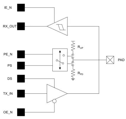
Block Diagram
Applications
- Every IC design that requires a higher/lower voltage tolerance
Deliverables
- GDSII
- LVS support
- Datasheet
- Documentation
- Integration guidelines and services
Technical Specifications
Foundry, Node
All foundries and processes
Maturity
Silicon proven
Availability
Immediate
Samsung
Silicon Proven:
4nm
TSMC
Silicon Proven:
22nm
,
28nm
,
28nm
HP
,
28nm
HPC
,
28nm
HPCP
,
28nm
HPL
,
28nm
HPM
,
28nm
LP
Related IPs
- General Purpose 10-bit DAC - 10 bits, 2MSPS, buffered output option - LFoundry 0.15µm LF150 CMOS
- General Purpose PLL for TSMC 152nm
- 28nm Wirebond IO library with dynamically switchable 1.8V/ 3.3V GPIO, 5V I2C open-drain, 1.8V & 3.3V analog, OTP program cell, and HDMI & LVDS protection macros - featured across a variety of metal stack and pad configuration options
- 3.3V Wide-Range General Purpose I/O Pad Set
- 3.3V Wide-Range General Purpose Staggered I/O Pad Set
- 1.8V 3.3V Tolerant General Purpose IO