Rambus PCIe Controller IP for USB4 is a configurable and scalable PCI Express controller soft IP designed for ASIC and FPGA implementations. It supports the PCI Express 5.0 specification, and implements the required features mandated by the USB4 Specification. The IP can be configured to support endpoint, root port, switch port, and dual-mode topologies, allowing for a variety of use models. The provided Graphical User Interface (GUI) Wizard allows designers to tailor the IP to their exact requirements, by enabling, disabling, and adjusting a vast array of parameters. Rambus PCIe Controller IP for USB4 enables designers to support tunneling of PCIe in USB4 Devices or Hosts for attaching PCIe devices either internally or externally. By implementing internal PCIe devices in their USB4 designs, designers can differentiate their USB4 ICs while reducing latency and power consumption.
PCIe Controller for USB4 Hosts and Devices, supporting PCIe Tunneling
Overview
Key Features
- PCI Express layer
- Designed to the USB4 Specification v1.0
- Follows PCIe 1.0 protocol, but can operate at any compatible speed
- Compliant with PCI-SIG Single-Root I/O Virtualization (SR-IOV) Specification
- Supports Endpoint, Root-Port, Dual-mode, Switch port configurations
- Supports up to 64 Physical Functions (PF), 512 Virtual Functions (VF)
- Supports AER, ECRC, ECC, MSI, MSI-X, Multi-function, crosslink, and other optional features
- Additional optional features include OBFF, TPH, ARI, LTR, IDO, L1 PM substates, etc.
- User Interface layer
- 512-bit or 256-bit transmit/receive low-latency user interface
- Up to 2 TLP per clock cycle (TLP chaining)
- User-selectable Transaction/Application Layer clock frequency
- Sideband signaling for PCIe configuration access, internal status monitoring, debug, and more
- Optional Transaction Layer bypass
- Integrity and Data Encryption (IDE)
- Implements the PCI Express IDE ECN
- Configurable IDE engine
- 256-bit or 512-bit data bus for PCIe IDE
- Supports containment and skid modes
- Supports early MAC termination
- Supports multi-stream
- Utilizes high-performance AES-GCM for encryption, decryption, authentication
- PCIe IDE TLP aggregation for 1, 2, 4, 8 TLPs
- PCIe IDE automatic IDE prefix insertion and detection
- PCIe IDE automatic IDE sync/fail message generation
- PCRC calculation & validation
- Efficient key control/refresh
- Bypass mode
Benefits
- Internal data path size automatically scales up or down (256-, 512- bits) based on max. link speed and width for reduced gate count and optimal throughput
- Dynamically adjustable application layer frequency down to 8Mhz for increased power savings
- Optional MSI/MSI-X register remapping to memory for reduced gate count when SR-IOV is implemented
- Configurable pipelining enables full speed operation on Intel and Xilinx FPGA, full support for production FPGA designs (when supported)
- Ultra-low Transmit and Receive latency (excl. PHY)
- Smart buffer management on receive side (Rx Stream) allows implementation of custom credit management schemes in the application logic
- Merged Replay and Transmit buffer enables lower memory footprint
- Advanced Reliability, Availability, Serviceability (RAS) features include LTSSM timers override, ACK/NAK/Replay/UpdateFC timers override, unscrambled PIPE interface access, error injection on Rx and Tx paths, recovery detailed status and much more, allowing for safe and reliable deployment of IP in mission-critical SoCs
- Optional Transaction Layer bypass allows for customer specific transaction layer and application layer
- Optional QuickBoot mode allows for up to 4x faster link training, cutting system-level simulation time by 20%
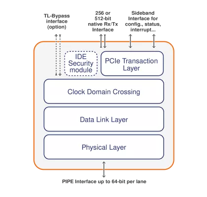
Block Diagram
Applications
- USB4 hubs for PC and automotive;
- USB4 hosts in PCs, laptops, gaming, TV and other chipsets;
- USB device adapters including USB4 to NVMe, USB4 to Audio/Video,
- USB4 eGPU and USB4 to Ethernet.
Deliverables
- IP files
- Verilog RTL source code
- Libraries for functional simulation
- Configuration assistant GUI
- Documentation
- PCI Express® Bus Functional Model
- Encrypted Simulation libraries
- Reference Designs
- Synthesizable Verilog RTL source code
- Simulation environment and test scripts
- Synthesis project & DC constraint files (ASIC)
- Synthesis project & constraint files for supported FPGA hardware platforms (FPGA)
Technical Specifications
Foundry, Node
Any
Availability
Available
Related IPs
- PCIe Controller for USB4 Hosts and Devices supporting PCIe Tunneling, with optional built-in DMA and configurable AMBA AXI interface
- PCIe Switch for USB4 Hubs, Hosts and Devices
- LPDDR Controller ASIL B Compliant supporting LPDDR5X, LPDDR5 and LPDDR4X for Automotive Applications
- LPDDR Controller ASIL B Compliant supporting LPDDR5, LPDDR4 and LPDDR4X for Automotive Applications
- LPDDR Secure Controller supporting LPDDR5, LPDDR4 and LPDDR4X with Advanced Features Package
- LPDDR Secure Controller supporting LPDDR5X, LPDDR5 and LPDDR4X with Advanced Features Package