The Universal NAND Flash Controller (UNFC) IP core is designed specifically to enable commodity Flash memory to be effectively used in enterprise storage applications requiring high reliability and large interconnect bandwidth. Using the pre-validated UNFC IP allows greatly reduced time-to-market for storage OEMs desiring higher IOPS benefitting from lower cost SLC, MLC & TLC / QLC NandFlash memory.
Universal NandFlash Controller
Overview
Key Features
- ONFI 5.X Compliant
- SLC / MLC / TLC
- SDR modes 0 to 5
- NVDDR modes 0 to 5
- NVDDR-2 modes 0 to 8
- NVDDR-3 modes 0 to 10
- NV-LPDDR-4 mode 0 to 10
- AXI or Avalon interface or RAM
- Up to ECC 84-errors / 1k block
- Configurable Data block size
Benefits
- Cost optimization
- High performance
- Reduced Time-To-Market by using validaded IP
- Full features
- Simulation testbench
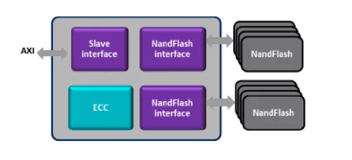
Block Diagram
Deliverables
- RTL design in verilog.
- Simulation testbench.
- Synthesis scripts for Xilinx, Altera and Design Compiler.
- Documentation.
Technical Specifications
Related IPs
- Universal Chiplet Interconnect Express (UCIe™) Controller
- Universal Asynchronous Receiver / Transmitter
- Universal Asynchronous Receiver / Transmitter
- 10G/2.5G/1G Multi-Speed Ethernet Controller IP for Automotive Applications
- 400G/800G High Speed Ethernet Controller MAC/PCS/FEC
- Universal Asynchronous Receiver Transmitter