The monitoring of process, voltage and temperature variations are critical to optimise power and performance for modern SoCs/ASICs, especially for advanced node and FinFET processes.
The agilePVT Sensor Subsystem is a low power integrated macro consisting of Process, Voltage, and Temperature sensors, and associated reference generator, for on-chip monitoring of a device's physical, environmental, and electrical characteristics.
Equipped with an integrated digital controller, the agilePVT Subsystem offers precise control over start-up and shutdown. Status monitors provide real-time feedback on the current state of the subsystem, ensuring optimal system performance over the full product lifecycle.
Agile Analog designs are based on tried and tested architectures to ensure reliability and functionality. Our design methodology is programmatic, systematic and repeatable leading to analog IP that is more verifiable, more robust and more reliable. Our methodology also allows us to quickly re-target our IP to different process options. We support all the major foundries including TSMC, GlobalFoundries, Samsung Foundry, Intel, and SMIC as well as other IC foundries and manufacturers. Please contact Agile Analog for further information.
PVT Sensor Subsystem
Overview
Key Features
- Temperature Sensor
- Measurement Range: -40oC to +125oC
- Accuracy (Uncalibrated) +/-5°C
- Accuracy (Calibrated)
- -20oC to +100oC = +/-2°C
- 0oC to +50oC = +/-0.5°C
- Silicon Area – Please contact Agile Analog
- Voltage Sensor
- Accuracy (Uncalibrated) 50mV
- Accuracy (Calibrated) 10mV
- Process Sensor
- In-chip monitoring of process variation
- Ring oscillator-based design to suit application requirements
- Scan-enabled to provide testability
- agilePVT Subsystem
- Start-up Time: Typ 20us
- Current Consumption: Max 25uA
- Industry standard digital interface
- Fully integrated macro
- Standard AMBA APB interface
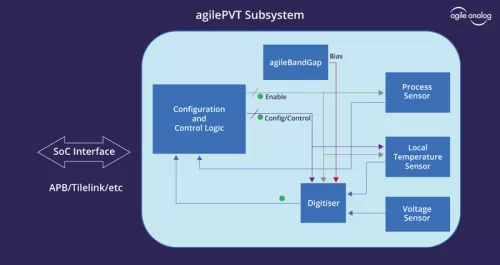
Block Diagram
Technical Specifications
GLOBALFOUNDRIES
Pre-Silicon:
12nm
,
14nm
,
14nm
LPE
,
14nm
LPP
,
20nm
LPM
,
22nm
,
22nm
FDX
,
28nm
,
28nm
FDSOI
,
28nm
HPP
,
28nm
LPH
,
28nm
SLP
,
32nm
,
40nm
LP
,
55nm
,
55nm
LPX
,
65nm
,
65nm
LP
,
65nm
LPe
,
90nm
,
90nm
LP
,
130nm
,
130nm
HP
,
130nm
LP
,
130nm
LV
,
180nm
,
180nm
LL
,
180nm
LL
,
180nm
LP
,
180nm
LP
Intel Foundry
Pre-Silicon:
16nm
SMIC
Pre-Silicon:
14nm
,
28nm
,
28nm
HK
,
28nm
HKC+
,
28nm
PS
,
40nm
LL
,
55nm
G
,
55nm
LL
,
65nm
LL
,
90nm
G
,
90nm
LL
,
110nm
G
,
130nm
EEPROM
,
130nm
G
,
130nm
LL
,
130nm
LV
,
150nm
G
,
150nm
LV
,
153nm
,
160nm
G
,
160nm
LL
,
180nm
EEPROM
,
180nm
G
,
180nm
LL
,
250nm
G
Samsung
Pre-Silicon:
4nm
,
5nm
,
7nm
,
8nm
,
10nm
,
11nm
,
14nm
,
28nm
FDS
,
28nm
LPH
,
28nm
LPP
TSMC
Pre-Silicon:
3nm
,
4nm
,
5nm
,
6nm
,
7nm
,
10nm
,
12nm
,
16nm
,
20nm
,
22nm
,
28nm
,
28nm
HP
,
28nm
HPC
,
28nm
HPCP
,
28nm
HPL
,
28nm
HPM
,
28nm
LP
,
40nm
G
,
40nm
LP
,
45nm
GS
,
45nm
LP
,
55nm
FL
,
55nm
G
,
55nm
GP
,
55nm
LP
,
55nm
NF
,
55nm
ULP
,
55nm
ULPEF
,
55nm
UP
,
65nm
G
,
65nm
GP
,
65nm
LP
,
80nm
,
80nm
GT
,
80nm
HS
,
85nm
,
90nm
FS
,
90nm
FT
,
90nm
G
,
90nm
GOD
,
90nm
GT
,
90nm
LP
,
90nm
zzz
,
110nm
G
,
110nm
HV
,
110nm
LVP
,
130nm
,
130nm
BCD
,
130nm
BCD+
,
130nm
G
,
130nm
LP
,
130nm
LV
,
130nm
LVOD
,
150nm
G
,
150nm
LV
,
160nm
G
,
160nm
LP
,
180nm
,
180nm
E
,
180nm
ELL
,
180nm
FG
,
180nm
G
,
180nm
LP
,
180nm
LV
,
180nm
ULL
Tower
Pre-Silicon:
130nm
,
180nm
,
180nm
,
180nm
,
500nm
UMC
Pre-Silicon:
14nm
,
22nm
,
28nm
,
28nm
HLP
,
28nm
HPC
,
28nm
HPM
,
28nm
LP
,
40nm
,
40nm
LP
,
55nm
,
65nm
LL
,
65nm
LP
,
65nm
SP
,
80nm
,
90nm
G
,
90nm
LL
,
90nm
SP
,
110nm
,
130nm
,
150nm
,
162nm