QDR IV XP PHY + Memory Controller
Overview
Atria Logic with its vast expertise and working experience for more than a decade in memory domains, brings a high speed PHY and Memory Controller for next generation memories introduced under the QDR consortium. Working at high speeds it garnishes the maximum speed of Stratix V FPGAs at 800MHz. De- skew training sequences, per-bit calibration and rate conversions at high speeds from uer interface (quarter rate) to memory interface (full rate) are some its features.
Key Features
- Standard: QDR IV XP (Extreme Performance) PHY and Memory Controller
- Frequency: Memory Interface : 800MHz
- User Interface : 200MHz
- Write Latency at Memory Interface : 5 Full Rate Cycles
- Read Latency at Memory Interface : 8 Full Rate Cycles
- Burst Length : 2 Words
- Calibration : Per-bit calibration for data, command and address on memory interface.
- Data Modes: x18 mode supported at 2 ports respectively. At one FR cycle 2 x (18+18) = 72b of data transferred.
- FPGA Platform: Stratix V FPGA
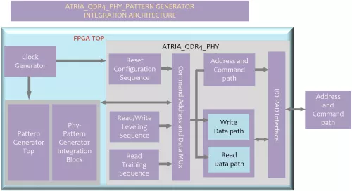
Block Diagram
Applications
- High performance networking and communication applications
- Servers
Deliverables
- FPGA specific netlist
- Complete HDLtestbench
- Test images
- Data Sheet and Users Guide
Technical Specifications
Availability
Now