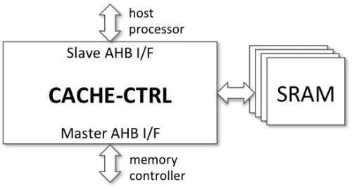
The CACHE-CTRL IP core is a flexible cache memory controller providing a 32-bit slave AHB processor interface and a 32-bit master AHB interface to the memory subsystem.
The cache controller core supports a four-way associative cache memory, and implements a Least Recently Used (LRU) replacement policy. The number of cache lines and the cache line width are configurable at synthesis time. The core only caches read accesses and invalidates the cached data if a write access to a cached memory location occurs.
Mapping the cache controller to any technology is straightforward, as the core does not require any special type of SRAM modules, only using standard, single-ported SRAMs. Furthermore, the design is scan-ready as it uses only rising-edge triggered flip-flops and contains no internal tri-states. Integration of the core is trouble-free, as the core uses standard 32-bit AHB interfaces, and supports clock gating.
The CACHE-CTRL core has been robustly verified and is silicon-proven.
AHB Cache Controller Core
Overview
Key Features
- Adds single or multilevel cache memory to originally cache-less deeply embedded processors, DSPs, or ASIPs. Improves access time and reduces bandwidth to DRAM, Flash or EEPROM memories; enables XIP without typical power or performance penalties.
- Cache Parameters
- Four-way set associative cache
- Least Recently Used (LRU) replacement policy
- Synthesis-time configurable:
- number of cache lines
- number of words per line
- 32-bit words
- Invalidates cache contents if a write access occurs
- Easy Integration & Implementation
- Works with any processor with a 32-bit AHB bus
- 32-bit AHB slave interface towards the processor
- 32-bit AHB master interface towards the memory system
- Uses four single-ported SRAMs: no special type of RAM is required
- Scan-ready design
- Supports clock gating
Block Diagram
Applications
- The CACHE-CTRL can be used to add single or multilevel cache memory to cache-less deeply embedded processors, DSPs, or ASIPs. This can decrease the read access time and bandwidth to a relatively slow or energy consuming memory resource like flash, EEPROM, or DRAM devices. For example it allows economical processors like the BA20, BA21, or BA22-DE to run code directly from an off-chip NOR-flash (XIP) while minimizing the typical performance and/or power penalties of off-chip access.
Deliverables
- Verilog RTL source code or targeted FPGA netlist
- Verification environment using System Verilog
- Assertions and Bus Functional Models
- Sample synthesis and simulation scripts
- User Documentation
Technical Specifications
Maturity
Production Proven
Availability
Now
Related IPs
- MIPI CSI-2 Controller Core
- MIPI DSI-2 Controller Core
- HBM2/2E Memory Controller Core
- ARC HS47D 32-bit, dual-issue processor core, ARCv2DSP ISA, with 100+ DSP instructions and I&D cache
- ARC HS57D 32-bit, dual-issue processor core and interconnect, ARCv3DSP ISA, with I&D cache
- ARC EM6 32-bit processor core with cache for embedded applications