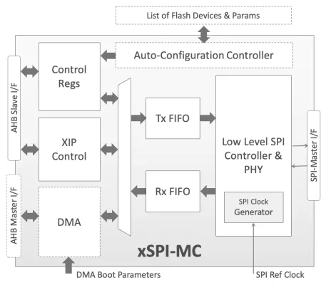
The xSPI-MC core is a versatile serial flash memory controller, which allows a system to easily detect and access the attached flash device or directly boot from it. The controller core supports most of the proprietary SPI protocols used by Flash devices vendors and is compatible with JEDEc’s eXpanded SPI (xSPI), and Xccela standards.
The core allows the system to interface with one or more serial flash devices in one of the following modes: a) in Slave mode by accessing its registers via an AHB slave interface; b) in DMA mode where the system programs the internal DMA engine and then the core accordingly drives its AHB master interface; c) in eXecute In-Place (XIP) mode where the core allows the system to directly access the SPI memory address space via an AHB slave interface; d) in Boot-Image copy mode where after reset the core will autonomously copy an amount of data (boot-image) from the SPI memory to the AHB address space (e.g. on a shadow RAM or DRAM) using its AHB master interface).
The core can work with single, dual, quad, twin-quad, and octal SPI flash devices. To enable use with flash devices from different vendors, the core offers two ways of configuring the device-specific parameters: a) via registers, where the system is responsible to identify the connected flash device and program the appropriate values to the core's registers; and b) by using the auto-configuration feature, where the core will autonomously identify the connected flash device and program itself accordingly. The auto-configuration functionality uses a user-provided memory that stores a list of automatically identifiable devices along with their features.
The xSPI-MC can be easily configured to match different application requirements. The data and address width of the AHB interfaces, instantiation of the DMA engine and the auto-configuration logic, the maximum number of Flash devices that the core supports, and the reset values for all configuration registers, are some of the design parameters that can be controlled by means of simple Verilog defines. Furthermore, the core can be easily implemented in any ASIC technology, as it features a synthesizable soft-PHY, and does not use any process-specific modules.
This core has been designed with industry best practices. It is LINT-clean and scan-ready, it has been verified through rigorous verification, and it is silicon-proven.
xSPI Flash Memory Controller
Overview
Key Features
- Compatible to most SPI protocols used by the NOR-Flash vendors including xSPI (JEDEC’s JESD251), and Xccela
- Single, Dual, Quad, Twin-Quad and Octal SPI lanes. Single and Dual Transfer Rate (STR and DTR)
- Programmable bit-length and number of SPI lanes used for command, address, latency (dummy cycle) and data. Programmable command encoding
- XIP - Allows AHB bus masters to read directly from the flash with zero software overhead.
- DMA – Optional DMA engine can be programmed to transfer data from/to system to/from the Flash device
- Boot-Image Copy - After reset the core uses its DMA engine to autonomously copy an amount of data from Flash to the AHB address space
- Slave Mode – System accesses core registers to transfer data to/from the Flash
- Flash Device-independent. The flash device parameters can be set at run time (either automatically or via configuration registers programming), or at synthesis time (via Verilog defines for reset values of all configuration registers)
- Process-independent, synthesizable, Soft PHY, enables easy mapping to any target technology.
- Zero software overhead with XIP and optional auto-configuration
- 32-bit and 64-bit AHB bus interfaces. Data-bus widths are configurable at synthesis timeThe
Benefits
- xSPI compliant
- XIP
- Optional DMA
- Small silicon footprint
- Soft PHY
Block Diagram

Deliverables
- Verilog source or FPGA netlist
- User Documentation
- Testbench and sample synthesis and simulation scripts
Technical Specifications
Maturity
Production Proven
Availability
Now