The USB 3.0 Device Upgrade IP enables designers in the PC, mobile, consumer and communication markets to bring significant power and performance enhancements to the popular USB standard while offering backwards compatibility with billions of USB-enabled devices currently in the market.
Arasan provides designers with a comprehensive, silicon-proven configurable digital USB 3.0 Device solution that conforms to the SuperSpeed specification. The USB 3.0 Device Upgrade is offered to customers with a USB 2.0 Device product interested in adding USB SuperSpeed (5Gbps) capability. It is designed to seamlessly upgrade existing USB 2.0 designs to the USB 3.0 specification for SoC development.
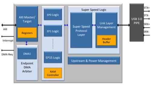
The Arasan USB 3.0 Device Upgrade provides a dedicated dual simplex, routable packet architecture for USB3.0 packet transfers, with a disable option for power savings. The Arasan USB 3.0 Upgrade IP supports all power management features as well as a dedicated link manager for each downstream port for increased efficiency. It includes a high performance scatter gather DMA that can be configured to access any endpoint through registers. Optionally, it can interface with an external DMA controller.
The USB 3.0 Device Upgrade IP core provides a PIPE interface for USB 3.0 support. The Arasan USB 3.0 IP utilizes a flexible system bus architecture that can support AXI, AHB, OCP or any custom system interface needed for existing SoC development. The system bus can also be replaced with a dedicated FIFO interface to reduce bus bandwidth issues. The IP core includes RTL code, test scripts and a test environment for complete design verification.
USB 3.0 Device Upgrade IP Core
Overview
Key Features
- USB 3.0 Compliance: SuperSpeed support: 5 Gbit/s
- 8/16/32 bit USB 3.0 PIPE interface
- Master DMA implementation for each endpoint with Scatter Gather support
- Optional slave DMA interface for external DMA implementations (auto mode)
- System bus Master/Target clock
- SuperSpeed Clock: 125/250/500 MHz
- Configurable up to 15 Tx and 15 Rx endpoints
- Configuration options: Bulk, control, isochronous, interrupt
- Dedicated control endpoint zero
- Configurable dual port RAM shared between endpoints
- Separate RAMs for upstream and downstream traffic
- All power states as specified in USB 3.0 specifications
- 32/64 bit AXI, AHB or OCP bus interface
- Seamless integration interface to Arasan PCI Express endpoint IP
Benefits
- Fully compliant core
- Premier direct support from Arasan IP core designers
- Easy-to-use industry standard test environment
- Un-encrypted source code allows easy implementation
- Reuse Methodology Manual guidelines (RMM) compliant verilog code ensured
Block Diagram
Deliverables
- RMM Compliant Synthesizable RTL design in Verilog
- Easy-to-use test environment
- Synthesis scripts
- Technical documents
Technical Specifications
Maturity
Silicon Proven
Availability
Now
Related IPs
- Complete memory system supporting any combinations of SDR SDRAM, DDR, DDR2, Mobile SDR, FCRAM, Flash, EEPROM, SRAM and NAND Flash, all in one IP core
- USB4.0 router, Certified USB 5G/10G and 20G Device controller
- BCH Encoder/Decoder IP Core
- USB 3.0 High/Full/Low-Speed Host + Device Controller IP
- DDR-I/II/III CONTROLLER IP CORE
- High-performance, low-power 2D composition IP core for embedded devices