Overview
The bi-directional LVDS is in production from 90nm CMOS to 16/12nm FinFET and taped out in 7nm FinFET. This LVDS I/O is highly programmable and is an excellent IO for FPGA to ASIC conversions.
LVDS-based Interfaces
Based on this versatile LVDS circuit and our robust PLLs and CDR architecture we developed multiple uni-directional and bi-directional parallel source-synchronous interfaces for Chip-chip and Video data transmission. These interfaces can comply with custom chip-chip (or chip-FPGA) requirements or standards including FPDLink, FastLVDS, miniLVDS, FPD Link, Camera Link and OpenLDI. A dynamic phase alignment and robust word alignment architecture enables data rates exceeding 190Mpixels/s (1.34Gb/s in each lane) for FPD-link and up to 3.3Gbps/lane in some cases.
Key Features
- TIA/EIA644A LVDS and sub-LVDS compatibility
- Receiver also compatible with LVPECL
- Operates over 2Gbps and up to 3Gb/s in some processes
- Trimmable on-die termination, can be enabled while Tx is operating for better signal integrity
- Independent LVCMOS input and output functions
Benefits
- Wide operating range
- High data rates
- Very flexible programmability
- Excellent signal integrity
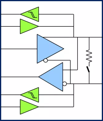
Block Diagram
Deliverables
- GDSII
- CDL Netlist (MG Calibre Compatible)
- Functional Verilog Model
- Liberty timing models (.lib)
- LEF
- Application Note with integration and production test guidelines
Technical Specifications
Foundry, Node
TSMC 5FF, 6FF, 7FF, 12FFC, 16FFC, 28HPC+, 40LP, 65LP, 90G
Maturity
Mass Production
Availability
Available Now
GLOBALFOUNDRIES
Silicon Proven:
40nm
LP
SMIC
Pre-Silicon:
40nm
LL
,
65nm
LL
,
90nm
G
TSMC
In Production:
5nm
,
7nm
,
12nm
,
16nm
,
28nm
HPC
,
28nm
HPCP
,
40nm
LP
,
65nm
LP
,
90nm
G
Silicon Proven:
6nm
,
22nm
,
28nm
HPM