The AHB Lite to AXI Bridge translates an AHB Lite bus transaction (read or write) to an AXI bus transaction. It is expected that the AXI clock and the AHB clock are derived from the same clock source, and that the period of the AHB Lite clock is an integer multiple of the AXI clock in the range [1,16].
Logic on two synchronous clock domains is used to accomplish the translation.
The AHB Lite logic is responsible for responding to transaction requests from the AHB Lite, and for generating AXI transactions based on transaction information from the AHB logic, and for presenting read data from the AXI subsystem back to the AHB Lite Master.
The AXI logic is responsible for generating AXI transactions based on transaction information from the AHB Lite logic, and for pacing the AXI transaction based on internal FIFO levels and on responses from the AXI Slave peripheral.
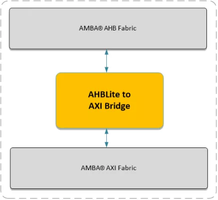
The AHB Lite to AXI Bridge acts as an AHB Lite Slave, and an AXI Master in an AXI/AHB subsystem. Typically, the AHB Lite to AXI Bridge has its AHB Lite interface connected to a Slave port on an AHB Lite Channel/Interconnect module, and its AXI interface connected to the Master port on an AXI Channel module.
AXI to AHB Lite Bus Bridge
Overview
Key Features
- Converts AHBLite Master transactions to AXI Master transactions
- Pseudo-synchronous clock domains
- FIFOs for BufferingAMBA® AXI-4 Compatible
- Multiple AXI Channels
- Off the shelf core supports 4 Masters and 8 Slaves
- Arbitration is done at each slave
- Other configurations are available
Block Diagram
Deliverables
- Verilog Source
- Complete Test Environment
- AXI Bus Functional Model
Technical Specifications
Maturity
Silicon Proven
Availability
Now