The multi-lane Multi-Protocol 10G PHY IP is part of a high-performance multi-rate transceiver portfolio, meeting the growing needs for low-power consumption and low latency in battery-operated consumer and mobile applications. The multi-protocol 10G PHY is small in area and provides low active and standby power while exceeding signal integrity and jitter performance of the PCI Express 3.1, SATA 6G and Ethernet standards.
The transmitter and receiver equalizers enable customers to control and optimize signal integrity and at-speed performance. Continuous Calibration and Adaptation (CCA) provides a robust performance across voltage and temperature variations during normal mode of operation. The PHY incorporates advanced power saving features such as L1 sub-states in-conjunction with power gating in standby mode of operation. The hybrid transmit drivers support low power voltage mode and high swing current mode, with optional I/O supply under drive to further save active power.
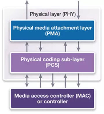
The PHY's Automatic Test Equipment (ATE) capabilities and optional wirebond packaging reduce the overall bill of materials (BOM) cost. The embedded bit error rate (BER) tester and internal eye monitor provide on-chip testability and visibility into channel performance. The PHY integrates seamlessly with the Synopsys Physical Sublayers and digital controllers/media access controllers (MACs) to reduce design time and to help designers achieve first-pass silicon success. These features reduce both product development cycles and accelerates time-to-market.
