The UHT-DSC-D core is a scalable, ultra-high throughput, advanced DSC 1.2b decoder, compliant to the VESA Display Stream Compression (DSC) 1.2b standard. It supports decoding of 4:4:4, 4:2:2 and 4:2:0 video streams, in 8 to 16 bits per component color depths.
The core is designed for enabling ultra-high frame rate SD, HD and Ultra HD video decoding up to 10K resolutions, even in medium-end ASIC or FPGA silicon. The scalability of this IP core enables highly cost-effective silicon implementations of applications that need to handle massive pixel rates and resolutions. The UHT-DSC-D is available for ASIC or Intel, Lattice, Microsemi and Xilinx FPGA and SoC based designs.
The UHT-DSC-D is very easy to use and integrate in a system, designed for using only internal memory blocks and with simple, fully controllable and FIFO-like, streaming input and output interfaces. It requires minimal host intervention as it only needs to be programmed once per video sequence. Once programmed, it can decode an arbitrary number of video frames without the need of any further intervention or assistance by the host system CPU.
Scalable Ultra-High Throughput DSC 1.2b Decoder
Overview
Key Features
- VESA DSC 1.2b Compliant, Complete and Standalone Operation
- Full compliance with the VESA DSC 1.2b specification
- Backwards compatible with VESA DSC 1.1
- RGB and YCbCr color space formats
- 8, 10, 12, 14 and 16 bits per color component dynamic range
- Native support for 4:4:4, 4:2:2 and 4:2:0 sampling formats
- Up to 16 slices per line
- Scalable architecture with configurable number of internal, parallel decoding engines
- 3 pixel/clock per decoding engine processing for 4:4:4 sampling format
- 6 pixels/clock per decoding engine processing for 4:2:2 and 4:2:0 sampling formats
- Operation without external memory
- Very low internal memory requirements (a few image lines)
- Ultra-low latency performance (sub-line latency)
- CPU/GPU-less, complete and standalone implementation
- Trouble-Free Technology Map and Implementation
- Self-contained RTL design
- No internal tri-states
- Strictly positive edge triggered design
- D-type only Flip-Flops
- Fully synchronous operation per clock domain
- Safe CDC transfers between clock domains
- No need for special timing constraints
- No false or multi-cycle paths within the same clock domain
- No CDC transfers that need to be specially constrained
- No other specially constrained timing paths
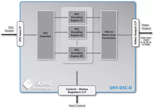
Block Diagram
Deliverables
- Clear text VHDL RTL source for ASIC designs, or pre-synthesized and verified Netlist for Intel, Lattice, Microsemi and Xilinx FPGA and SoC devices
- Extensive documentation
- Bit Accurate Model (BAM) with optional Test Vector generation functionality
- Self-checking testbench environment
- Sample BAM scripts
- Synthesis scripts
- Simulation scripts
- Place & Route scripts for FPGAs
Technical Specifications
Related IPs
- Scalable Ultra-High Throughput DSC 1.2b Encoder
- Scalable UHD JPEG Encoder – Ultra-High Throughput, 8/10/12-bit per component and CBR video encoding
- Scalable UHD JPEG Decoder – Ultra-High Throughput, 8/10/12-bit per component
- Scalable UHD H.264 Encoder - Ultra-High Throughput, Intra frames (IDR) encoding
- Scalable UHD H.264 Encoder - Ultra-High Throughput, Light Motion Estimation engine
- Scalable UHD H.264 Encoder - Ultra-High Throughput, Full Motion Estimation engine