PCIe 3.0, 2.1, 1.1 Controller with the PHY Interface for PCI Express (PIPE) specification and native user interface support
Overview
Rambus PCIe 3.0 Controller is a highly configurable PCIe 3.0 interface Soft IP designed for ASIC and FPGA implementations supporting endpoint, root port, switch, bridge and advanced features such as SR-IOV, multi-function, data protection (ECC, ECRC), ATS, TPH, Advanced Error Reporting (AER) and more. Rambus PCIe 3.0 Controller is the industry’s PCIe IP of choice for enterprise-class applications requiring the highest performance, reliability, and flexibility.
Key Features
- Complies with the PCI Express® Base 3.0 Specification, rev.3.1
- Supports Endpoint, Root-Port, Dual-Role, Switch configurations
- Supports x16, x8, x4, x2, x1 at Gen3, Gen2, Gen1 speeds
- Implements one Virtual Channel
- Maximum payload size of up to 4KB
- Built-in clock domain management
- User Interface
- Tx/Rx for data
- 256-bit data path, user-selectable frequency
- Sideband interfaces for configuration, debug, monitoring, advanced features
- TL bypass interface for switch/bridge implementations
- PHY Interface
- PIPE 3.0 compliant
- 32bit/250MHz in Gen3 mode
- 16-bit mode supported
- Advanced features include
- Multi-function
- Advanced Error Reporting (AER)
- Data Protection (ECC,ECRC)
- End-End TLP prefixes
- TPH
- OBFF
- MSI, MSI-X
- ASPM and legacy power management
- Lane Reversal
- Hot Plug
- Atomic operations
- Virtualization ready with SR-IOV and ATS /ARI
- L1 PM substate with CLKREQ
Benefits
- Engineered for both ASIC/SoC and FPGA implementations. Allows seamless migration from FPGA prototyping design to ASIC/SoC production design with same RTL. Fully timing closed on leading edge FPGA from Altera and Xilinx
- Multi-mode PIPE support enables proven interoperability with broad range of PHY IP at various foundries and process nodes
- Demonstrated SR-IOV support allows seamless integration into virtualized environments.
- Support for advanced Low Power states enables lower power consumption in energy-conscious applications
- Configurable FIFO based user interface with clock-domain-crossing provides maximum interfacing flexibility and throughput.
- Extensive data integrity features provide data protection on entire data path for storage and other data critical applications
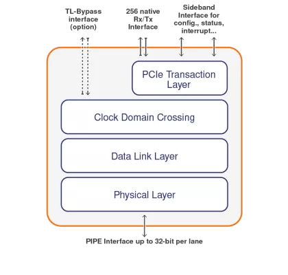
Block Diagram
Applications
- HPC,
- Cloud Computing,
- AI,
- Machine Learning,
- Enterprise,
- Networking,
- Automotive,
- AR/VR,
- Test and Measurement
Deliverables
- Verilog RTL,
- Supporting Documentation
Technical Specifications
Foundry, Node
Any
Maturity
In production
Availability
Available
GLOBALFOUNDRIES
In Production:
28nm
SLP
,
40nm
LP
,
55nm
,
65nm
,
65nm
LP
,
65nm
LPe
,
90nm
,
90nm
LP
,
130nm
,
130nm
HP
,
130nm
LP
,
130nm
LV
Pre-Silicon: 28nm SLP , 40nm LP , 55nm , 65nm , 65nm LP , 65nm LPe , 90nm , 90nm LP , 130nm , 130nm HP , 130nm LP , 130nm LV
Silicon Proven: 28nm SLP , 40nm LP , 55nm , 65nm , 65nm LP , 65nm LPe , 90nm , 90nm LP , 130nm , 130nm HP , 130nm LP , 130nm LV
Pre-Silicon: 28nm SLP , 40nm LP , 55nm , 65nm , 65nm LP , 65nm LPe , 90nm , 90nm LP , 130nm , 130nm HP , 130nm LP , 130nm LV
Silicon Proven: 28nm SLP , 40nm LP , 55nm , 65nm , 65nm LP , 65nm LPe , 90nm , 90nm LP , 130nm , 130nm HP , 130nm LP , 130nm LV
Renesas
In Production:
40nm
,
55nm
,
90nm
Pre-Silicon: 40nm , 55nm , 90nm
Silicon Proven: 40nm , 55nm , 90nm
Pre-Silicon: 40nm , 55nm , 90nm
Silicon Proven: 40nm , 55nm , 90nm
SMIC
In Production:
40nm
LL
,
55nm
G
,
55nm
LL
,
65nm
LL
,
90nm
G
,
90nm
LL
,
110nm
G
,
130nm
G
,
130nm
LL
,
130nm
LV
Pre-Silicon: 40nm LL , 55nm G , 55nm LL , 65nm LL , 90nm G , 90nm LL , 110nm G , 130nm G , 130nm LL , 130nm LV
Silicon Proven: 40nm LL , 55nm G , 55nm LL , 65nm LL , 90nm G , 90nm LL , 110nm G , 130nm G , 130nm LL , 130nm LV
Pre-Silicon: 40nm LL , 55nm G , 55nm LL , 65nm LL , 90nm G , 90nm LL , 110nm G , 130nm G , 130nm LL , 130nm LV
Silicon Proven: 40nm LL , 55nm G , 55nm LL , 65nm LL , 90nm G , 90nm LL , 110nm G , 130nm G , 130nm LL , 130nm LV
TSMC
In Production:
40nm
G
,
40nm
LP
,
45nm
GS
,
45nm
LP
,
55nm
GP
,
55nm
LP
,
65nm
G
,
65nm
GP
,
65nm
LP
,
80nm
,
80nm
GT
,
80nm
HS
,
90nm
G
,
90nm
GOD
,
90nm
GT
,
90nm
LP
,
90nm
zzz
,
110nm
G
,
110nm
LVP
,
130nm
G
,
130nm
LP
,
130nm
LV
,
130nm
LVOD
Pre-Silicon: 28nm HP , 28nm HPL , 28nm HPM , 28nm LP , 40nm G , 40nm LP , 45nm GS , 45nm LP , 55nm GP , 55nm LP , 65nm G , 65nm GP , 65nm LP , 80nm , 80nm GT , 80nm HS , 90nm G , 90nm GOD , 90nm GT , 90nm LP , 90nm zzz , 110nm G , 110nm LVP , 130nm G , 130nm LP , 130nm LV , 130nm LVOD
Silicon Proven: 40nm G , 40nm LP , 45nm GS , 45nm LP , 55nm GP , 55nm LP , 65nm G , 65nm GP , 65nm LP , 80nm , 80nm GT , 80nm HS , 90nm G , 90nm GT , 90nm LP , 90nm zzz , 110nm G , 110nm LVP , 130nm G , 130nm LP , 130nm LV , 130nm LVOD
UMC
In Production:
40nm
,
40nm
LP
,
65nm
LL
,
65nm
LP
,
65nm
SP
,
90nm
G
,
90nm
LL
,
90nm
SP
Pre-Silicon: 40nm , 40nm LP , 65nm LL , 65nm LP , 65nm SP , 90nm G , 90nm LL , 90nm SP
Silicon Proven: 40nm , 40nm LP , 65nm LL , 65nm LP , 65nm SP , 90nm G , 90nm LL , 90nm SP
Pre-Silicon: 40nm , 40nm LP , 65nm LL , 65nm LP , 65nm SP , 90nm G , 90nm LL , 90nm SP
Silicon Proven: 40nm , 40nm LP , 65nm LL , 65nm LP , 65nm SP , 90nm G , 90nm LL , 90nm SP
Related IPs
- PCIe 2.1 Controller with the PHY Interface for PCI Express (PIPE) specification and native user interface support
- PCIe 3.0, 2.1, 1.1 Controller supporting Root Port, Endpoint, Dual-mode Configurations, with AMBA AXI User Interface
- USB 3.2 Gen2x2 with PIPE 4.3 and USB2.0 with UTMI+ interface
- VME System Controller with AXI4 user interface and 2eSST support
- PCIe Controller for USB4 supporting up to PCIe 4.0 with AMBA interface
- SuperSpeed USB 3.0 Dual Role Device Controller, Configurable for SSIC and HSIC