Lowest latency and highest data rates for data-intensive applications
The latest, the Cadence Denali PHY IP for GDDR6, is comprised of architectural improvements drawn from previous-generation DDR PHYs and Cadence’s 10G, 16G, and 25G SerDes, achieving breakthrough performance, low energy per bit, and low area relative to the bandwidth provided. This application-optimized PHY IP can achieve speeds up to 16Gbps across its full-rated range of process, voltage, and temperature, while extensions up to 20Gbps are possible with modifications. The PHY IP for provides a low bit error rate (BER) that can improve bandwidth utilization and maximum latency. The PHY IP is designed to be compatible with standard PCB materials like FR4 up to 16Gbps. The PHY IP is developed by experienced teams with industryleading domain expertise and extensively validated with multiple hardware platforms. It is engineered to quickly and easily integrate into systems on chip (SoCs), and is verified with the Cadence Denali Controller IP for GDDR6 as part of a complete memory subsystem solution.
GDDR6 PHY for Samsung
Overview
Key Features
- Single configuration supports one GDDR6 device per channel (coplanar) or two GDDR6 devices per channel (clamshell)
- Memory controller interface uses DFI 5.0-like standard with extensions for GDDR6
- Internal and external datapath loop-back modes
- Per-bit DFE, CTLE, and FFE equalization
- DFI PHY Independent Mode for initialization and training
- Adaptive and continuous timing recovery
- Transmit crosstalk cancelation of immediate neighbors
- 8:1 memory:controller clock ratio for easy controller timing closure
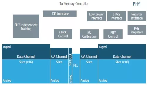
Block Diagram
Applications
- Communications,
- Consumer Electronics,
- Data Processing,
- Industrial and Medical,
- Military/Civil Aerospace
Deliverables
- GDS II macros with abstract in LEF
- Verilog post-layout netlist
- STA scripts for use at chip or standalone PHY levels
- Liberty Timing model
- SDF for back-annotated timing verification
Technical Specifications
Foundry, Node
Samsung 7nm, 14nm
Maturity
Available on request
Samsung
Pre-Silicon:
7nm
,
14nm
Related IPs
- USB-C 3.1/DP TX PHY for Samsung 11LPP, North/South Poly Orientation
- USB-C 3.1/DP TX PHY for Samsung 14LPP, North/South Poly Orientation
- USB-C 3.1/DP TX PHY for TSMC 12FFC, North/South Poly Orientation
- USB-C 3.1/DP TX PHY for TSMC 16FFC, North/South Poly Orientation
- USB-C 3.1/DP TX PHY for TSMC 7FF, North/South Poly Orientation
- USB 3.0 PHY - Samsung 28LPP18 x1, OTG, North/South (vertical) poly orientation