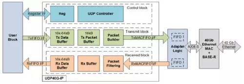
UDP40G IP core implements UDP/IP stack and designs to connect with 40 Gb Ethernet MAC and PCS/PMA (BASE-R) module through adapter logic. The reference design uses 40G EMAC and PCS/PMA from Xilinx. The user interface of UDP40G IP uses the simple standard interface, so User logic can transfer 40 Gb Ethernet data with network equipments by designing small logic.
User interface could be split into two groups, i.e. control signals and data signals. Control signals are designed by using general register interface while data signals are designed by using 256-bit general FIFO interface.
Register interface is used to set network parameters of UDP40G IP and the target device such as IP address and port number. Also, it is applied to start sending data operation and the control parameters for sending data such as transfer size and packet size.
Data interface of user logic is 256-bit FIFO interface for both Tx and Rx direction. User can design simple logic or connect to FIFO for connecting to UDP40G IP.
To initialize system, user needs to set up all network parameters of UDP40G IP and the target device, i.e. MAC address, port number, and IP address through register interface. After finishing initialization, UDP40G IP is ready to send or receive data with the target device. To send data, user sets command register and then transfer data to UDP40G IP until finishing. UDP40G IP creates UDP/IP packet which includes the user data and forwards to Ethernet MAC, following the parameters. Otherwise, when the new packet is received and the header in the packet is valid (matched to the parameters), UDP40G IP extracts only the data to return to user.
UDP40G-IP Core
Overview
Key Features
- UDP/IP stack implementation
- Support IPv4 protocol
- Support one session per one UDP40G IP (Multisession implemented by using multiple UDP40G IP)
- Support Jumbo frame
- Simple user interface for control signals by standard register interface
- Simple user interface for data signals by 256-bit standard FIFO interface
- Transmit packet size must be aligend to 32-byte to match Tx FIFO interface
- Total received data must be aligend to 32-byte to read from Rx FIFO interface
- Adjustable transmit/receive buffer size to optimize resource and performance
- 256-bit FIFO interface with Ethernet MAC
- At least 200 MHz is recommended for clock input to UDP40G IP
- Reference design available on ZCU102, ZCU106, and KCU105 evaluation board
- Support IP fragmentation feature
Block Diagram