Why Chip Design AI Benchmarks Must Go Beyond Functional Correctness

Demand for custom silicon is rising as physical AI, data centers, automotive systems, and edge devices require architectures optimized for specific workloads, memory bandwidth, latency, and energy efficiency. Delivering these designs requires teams to coordinate heterogeneous compute blocks, complex interconnects, and multiple domains while closing increasingly demanding power, performance, and area (PPA) targets.
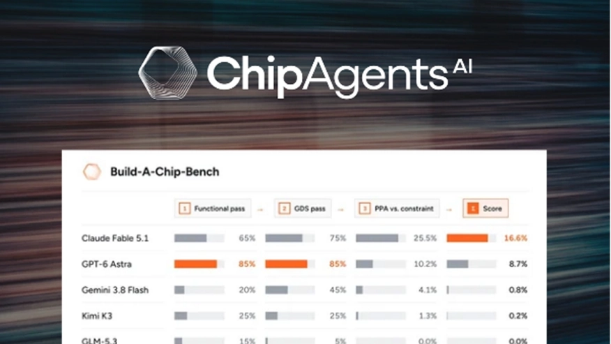 AI offers a way to expand engineering capacity and accelerate chip design cycles. Design and verification engineers already use AI to generate test cases, assist debugging, and implement portions of RTL. The next question is whether these capabilities can extend across an entire design flow, where decisions made during RTL implementation must hold up through verification, synthesis, and physical design.
To help answer that question, ChipAgents developed Build-A-Chip-Bench with NVIDIA to evaluate AI agents across the end-to-end digital IC design flow, from specification through physical implementation and verified Graphic Design System (GDS). The benchmark evaluates AI agents on realistic, demanding tasks that connect individual design steps to a measurable engineering outcome.
To read the full article, click here
Related Semiconductor IP
- LPDDR6 PHY
- UMC 55nm ULP 3.3V Temperature Sensor
- High-Throughput Multi-Channel DMA Controller
- Configurable Multi-Channel DMA Controller
- Fixed-Channel Multi-Channel DMA Controller
Related Blogs
- Hardware security verification must go beyond functional testing
- Securing AI at Its Core: Why Protection Must Start at the Silicon Level
- Reimagining Chip Design - From Spec to Signoff with Cadence AI Super Agents
- Beyond PCIe Compliance: Why Stress Testing Is Crucial for Edge AI Deployments