Vendor: Nordic Semiconductor Seattle Category: SRAM

Single Port, Voltage Scaling, High Speed SRAM Memory Compiler on GF22FDX+

Single Port SRAM w/dedicated Standby mode, optional array source biasing & separate array/periphery power supplies for ultra low leakage - Bit Cell: L110

GlobalFoundries 22nm FDX+ Available on request View all specifications

Overview

 Single Port, Voltage Scaling, High Speed SRAM Memory Compiler on  GF22FDX+ - Bit Cell: L110 - Power Supply (V): 0.5V to 0.8V

Technology GF 22nm FDX-PLUS
Bit Cell 6T L110, 0.110 µm²
Periphery VDD 0.5 / 0.65 / 0.8 V
Array VDM 0.8 V
Temperature -40°C to +125°C
Power Mesh
# Metal Layers 4
Modes Functional / Scan / Sleep
Interface Command line (mscinsgen)
Max Instance 1.2 Mb (1248 Kb)
Min Instance 1 Kb
Word Width 8 - 144 bits
Word Depth 64 - 16384 words
Banks 1, 2, 3, 4
Column Fold 4, 8
Speed Fast / Faster
Write Enable Optional bit or byte
Error Detection SECDED or Parity
EDA Views (Partial List)  
GDSII Layout LEF
LVS SPICE Netlist Liberty: NLDM / CCS / LVF
Behavioral Verilog + Testbench Structural Verilog
UPF Power Models ATPG: generic / Tessent
Tessent MBIST Control PDF / Text Datasheets
Bitmap (x,y) APL Power Model
Voltus Power Grid Scripts Hierarchical LVS cell list

Key features

  • Voltage Scaling: Periphery VDD supports 0.5 V, 0.65 V, or 0.8 V while the SRAM array operates at 0.8 V (VDM); level translation is internal to the macro.
  • High-Speed Architecture: Up to four banks shorten bit lines and improve timing; I/O is placed on the instance edge for routing usability.
  • Low-Leakage Retention: Dedicated sleep mode uses optional array source biasing and separate array/periphery supplies so the periphery can be powered off while data is retained.
  • Bit Cell: Uses GLOBALFOUNDRIES 22FDX-PLUS low-leakage 6T L110 bit cells with a drawn area of 0.110 µm².
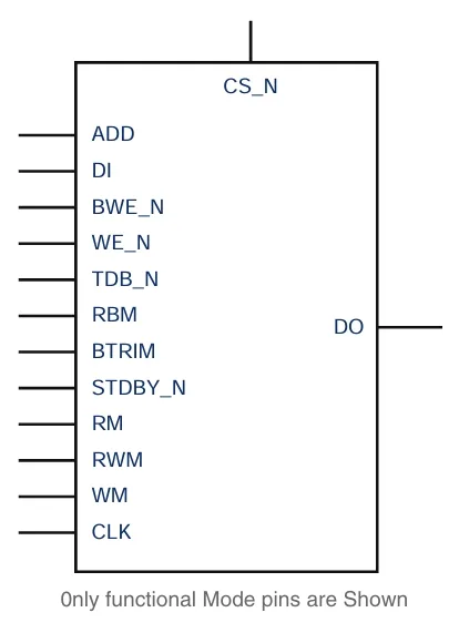
  • Timing Margin Control: RWM, RM, and WM inputs provide selectable read/write timing margins, including fast-read and fast-write settings.
  • Body Bias Support: Periphery body-bias supplies are compatible with RacyIC active body bias; optional RBM control adjusts bit-cell speed/leakage.
  • Bit / Byte Write: Optional bit write enables independent writes to any subset of a word; programmable byte-wide write enable reduces control-pin count.
  • Error Protection: Optional SECDED supports single-bit correction and dual-bit detection; parity error detection is also available.
  • Speed Grades: Fast supports the full instance-size range; Faster provides the highest speed with tighter instance-size limits.

Block Diagram

Silicon Options

Foundry Node Process Maturity
GlobalFoundries 22nm FDX+ Available on request

Specifications

Identity

Part Number
SP-ULX-GF22FDX-PLUS
Vendor
Nordic Semiconductor Seattle
Type
Silicon IP

Files

Note: some files may require an NDA depending on provider policy.

Provider

Learn more about SRAM IP core

Frequently asked questions about SRAM IP cores

What is Single Port, Voltage Scaling, High Speed SRAM Memory Compiler on GF22FDX+?

Single Port, Voltage Scaling, High Speed SRAM Memory Compiler on GF22FDX+ is a SRAM IP core from Nordic Semiconductor Seattle listed on Semi IP Hub. It is listed with support for globalfoundries Available on request.

How should engineers evaluate this SRAM?

Engineers should review the overview, key features, supported foundries and nodes, maturity, deliverables, and provider information before shortlisting this SRAM IP.

Can this semiconductor IP be compared with similar products?

Yes. Buyers can compare this product with similar semiconductor IP cores or IP families based on category, provider, process options, and structured technical specifications.

×
Semiconductor IP