Beyond PCIe Compliance: Why Stress Testing Is Crucial for Edge AI Deployments
Passing PCI Express (PCIe) compliance is different from being ready for the field. A PCIe link can clear every test in a controlled lab environment and still develop margin problems six months into deployment. That’s because a compliance traffic generator isn’t designed to replicate real-world operating conditions, such as thermal stress, electrical noise, and the kind of bursty inference traffic that arises from edge AI systems constantly scaling power and performance. While compliance provides assurance that the design meets the specification, it doesn't tell you how much margin remains before it disappears once the device is in the field. Stress testing closes this gap.
Compliance and Stress Testing Answer Different Questions
Compliance testing validates conformance: does this device interoperate correctly within the ecosystem and meet specification-defined electrical parameters? It is a structured, reproducible exercise designed to produce consistent results under consistent conditions, which is both its value and its limitation.
Stress testing asks a different question: how much margin is there, and what happens when real operating conditions begin to consume it? Two examples of potential failure modes illustrate why this distinction matters.
First: If an implementer has a compliant design with only a modest margin at room temperature and nominal supply can consume that margin once the junction temperature rises under sustained load. It is possible to pass compliance under nominal conditions, but fail in real-world scenarios.
Second: A hypothetical device that recovers cleanly from a single L1 exit during compliance testing can still accumulate intermittent CRC errors after repeated power-state cycling. This is the kind of constant ramp-up and ramp-down behavior real inference workloads impose on deployed systems.
These scenarios are not edge cases but are normal operating cases. Compliance testing is not intended to catch them. That is where stress testing comes in. Compliance testing is necessary, but not sufficient.
What Real Stress Testing Actually Covers
Stress testing is a validation philosophy. At the device level, it means characterizing behavior beyond the compliance test points. These include receiver jitter tolerance swept across degraded input conditions, transmitter output across supply and temperature corners, and device-level qualification tests such as ESD, latch-up, and HTOL—the last of which specifically validates that parametric performance doesn't drift under sustained thermal stress over the product's lifetime.
At the system level, the scope expands to encompass the operating conditions encountered in real deployments. Lane-width variation matters because crosstalk and skew behavior differ across x1, x4, and x8 configurations in ways that single-lane compliance won't expose. Speed negotiation testing, which entails exercising fallback and upgrade transitions between PCIe generations under realistic channel and loading conditions, validates LTSSM behavior where it's most likely to develop intermittent issues. Cold and warm boot cycling, across hundreds to thousands of iterations, approximates long-field initialization behavior far more closely than a one-shot compliance bring-up sequence.
Long-duration BER testing deserves particular attention. A link that shows zero errors over a short compliance measurement window can still have a non-zero BER floor that becomes statistically significant over months of continuous operation. Characterizing that floor across different channels and with intentionally degraded signal conditions is the only way to know whether the design has real margin or just hasn't been stressed long enough.
Many of these conditions extend beyond the baseline scope of PCIe compliance validation. To address that gap, Cadence developed additional internal stress-testing methods that evaluate PCIe IP under broader electrical, functional, and system-level conditions. These methods build on standard compliance and qualification practices, extending them into more realistic operating scenarios to improve confidence in field reliability.
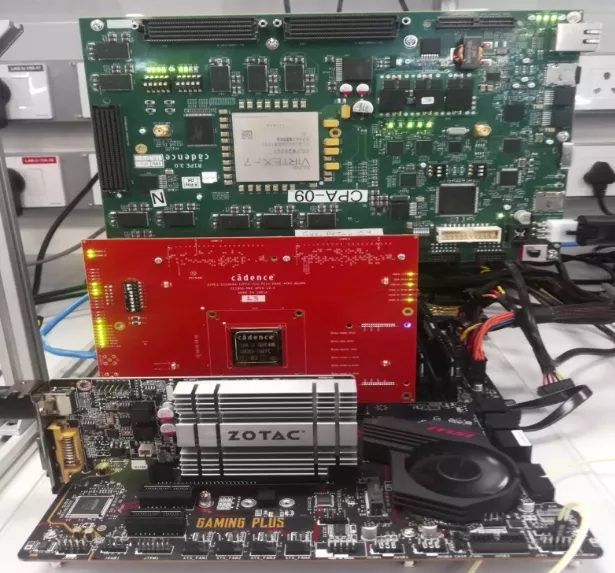
Figure 1: Cadence generic multi-lane PCIe validation test setup
Edge AI Makes the Problem Real
Take a concrete deployment: industrial edge AI servers built on PCIe 4.0 platforms. These systems, used in factory automation, logistics, and machine vision, run continuously in thermally variable enclosures, handle sustained multi-sensor inference loads, and operate with little to no local maintenance support. Operating ranges of -20°C to 60°C are standard in these environments. Power-state transitions occur constantly as the NPU idles between inference requests and wakes under load. The PCIe links connecting accelerators, NVMe storage, and high-speed I/O are doing real work in conditions that compliance testing wasn’t designed to replicate.
When a PCIe link develops problems in a data center, the issue is typically visible and diagnosable. Errors are logged, and telemetry is available. Performance degradation can be correlated with system events, and remediation can often be planned without immediate physical access due to redundancy and centralized monitoring.
In a distributed edge deployment, the failure mode is rarely that cooperative. Symptoms tend to be intermittent and might include unexpected inference latency, throughput variance that defies easy explanation, and sporadic link recovery events that don't trigger hard faults but gradually degrade system behavior over time. The root cause is hard to reproduce remotely, and the fix requires physical access to hardware that may be geographically scattered across hundreds or thousands of sites.
The cost of a thin‑margin implementation with limited electrical and timing headroom under real operating conditions can scale quickly with deployment volume, diagnostic effort, and time‑to‑resolution in edge AI environments.
From Compliance to Field Reliability
Compliance is only part of the story. It tells you whether a design meets the standard under controlled conditions. Stress testing goes further, showing how much operating margin remains once thermal cycling, power-state transitions, extended uptime, workload bursts, and channel variation begin to consume it.
For edge AI, where operating environments are harsher and field lifetimes are longer, that difference directly impacts link stability, diagnosability, and long‑term system reliability. This isn’t an abstract quality metric. It determines whether systems behave predictably over years of deployment or slowly degrade in ways that are difficult and costly to diagnose.
Cadence validates PCIe IP across generations with stress testing built into the process. Compliance is only a baseline, while margin characterization is the proof of field readiness.
Learn more about Cadence PCIe IP Solutions for building field‑ready edge AI systems.
Related Semiconductor IP
- Controller for PCIe
- Simulation VIP for PIPE PHY
- Simulation VIP for PCIe
- PCI Express Verification IP
- Scalable Switch Intel® FPGA IP for PCI Express
Related Blogs
- PCIe 6.x: Synopsys IP Selected as First Gold System for Compliance Testing
- Rethinking Edge AI Interconnects: Why Multi-Protocol Is the New Standard
- High-Speed Test IO: Addressing High-Performance Data Transmission And Testing Needs For HPC & AI
- Accelerating PCIe Gen6 L0p Verification for AI & HPC Designs using Synopsys VIP
Latest Blogs
- Embedded Security explained: Secure boot for embedded systems
- World's First Standards-Compliant 112G PHY IP for Linear Optics: A Turning Point for AI Interconnects
- One Key for Every Door: How Aliro Extends the UWB Digital Key Beyond the Car
- Reprogrammable Post-Quantum Security for SoCs: Why Crypto-Agility Matters
- Designing the Beam Steering Core for a C-Band AESA: A Look at VSI's VBF0644 GaAs Beamformer IC