Design and Development of a Neuromorphic Silicon Suite: PVT Sensing, Stochastic LIF Inference, On-Chip STDP Learning, and Crossbar Programming
By Poornima Kumaresan and Santhosh Sivasubramani
Intrinsic Lab, Centre for Sensors, Instrumentation and Cyber-Physical System Engineering (SeNSE), Indian Institute of Technology Delhi, New Delhi 110016, India
Abstract
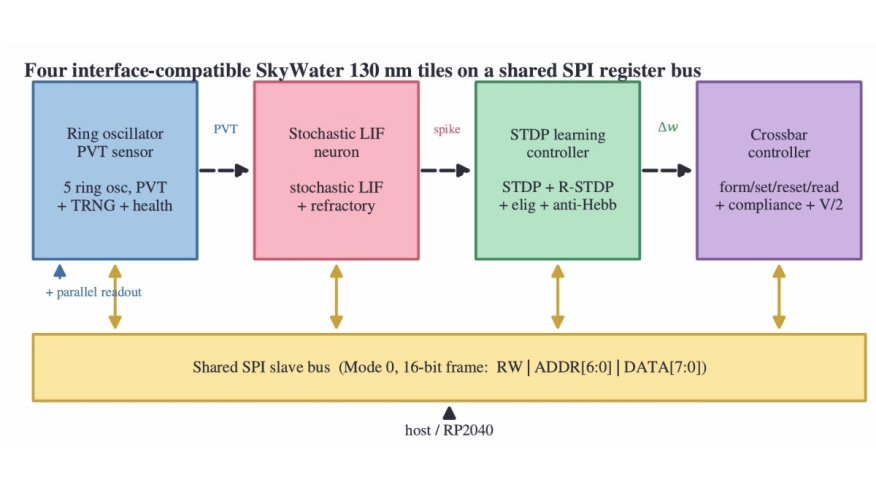
Edge neuromorphic systems need compact, configurable hardware that combines probabilistic inference, local learning, and an interface to emerging analogue memory. We present four interface-compatible digital IP blocks implemented as standard-cell CMOS on the SkyWater 130 nm process: a process, voltage and temperature (PVT) sensor built from five selectable ring oscillators that also provides a jitter-based true-random-number generator and a frequency-bounds health monitor; a stochastic leaky integrate-and-fire (LIF) neuron with a configurable LFSR, a programmable activation table, and a refractory period; an on-chip spike-timing-dependent plasticity (STDP) controller with a programmable curve and reward-modulated, eligibility-trace, and anti-Hebbian modes; and a memristive-crossbar controller supporting forming, set, reset, read, and automated current-voltage sweep with current-compliance limiting and half-select biasing. All four blocks share a common serial peripheral interface (SPI) register file; the sensor also exposes a parallel readout. Each occupies a single tile at a 50 MHz target. The suite was verified with 99 cocotb tests at register-transfer and gate level (all passing) and taken through an open standard-cell flow, then submitted for tapeout via the Tiny Tapeout shared-silicon programme. Mapped to the open cell library, each block occupies a post-synthesis cell area of 9.3 to 10.6 thousand square micrometres, places at 61 to 70 per cent tile utilisation, meets the 50 MHz constraint with positive setup and hold margin after clock-tree synthesis, and draws an estimated 0.64 to 0.70 mW under a default switching-activity assumption. The contribution is a coherent, openly released set of building blocks unified by one register interface and one verification flow. All results are from simulation and the implementation flow; no fabricated silicon is reported.
To read the full article, click here
Related Semiconductor IP
- Ultra-low jitter, low-power ring-oscillator-based PLL-3GHz-4GHz
- Image Warping IP
- Image Warping IP
- ML-KEM-X Post-Quantum Cryptography Core
- AXI5 to/from AXI4 Bridge
Related Articles
- ITP-STDP: An Intrinsic-Timing Power-of-Two Learning Engine for On-Chip SNN Training
- Importance of Dynamic Programming for Achieving Hard Breakdown in Anti-Fuse Technology
- All-in-One Analog AI Hardware: On-Chip Training and Inference with Conductive-Metal-Oxide/HfOx ReRAM Devices
- Bare-Metal RISC-V + NVDLA SoC for Efficient Deep Learning Inference
Latest Articles
- Vectorizing Quantum Control: A RISC-V Vector Extension Architecture for Scalable Qubit Systems
- FlexViT: A Flexible FPGA-based Accelerator for Edge Vision Transformers
- LIB-TRAP: Standard Cell Library Hardware Trojan Risk Assessment and Prevention
- Exploring Side-Channel Protections in Hardware Implementations of PQC ML-KEM Verification
- CVA6-RT: an Open-Source Time-Predictable RV64 Processor for Mixed-Criticality Systems