3.6 Kbit EEPROM IP
28 pages × 8 words × 16 bit, parallel word write, single high-voltage pulse erase/program with automatic sequencing.
Overview
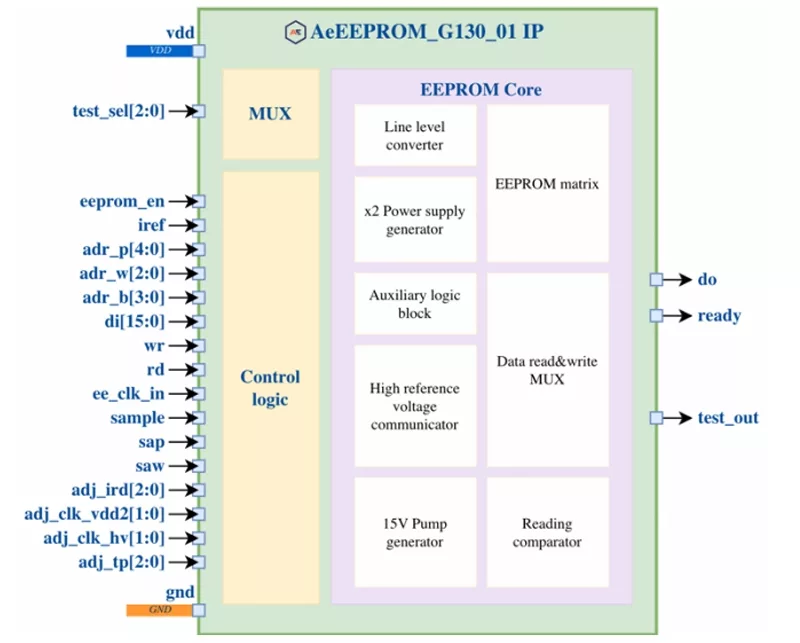
AeEEPROM_G130_01 is a silicon-proven, non-volatile electrically erasable programmable read-only memory (EEPROM) IP with 3.6Kbit capacity, organized as 28 pages of 8 words by 16 bits with parallel word write and single-bit read output. Data is written and erased by a single high-voltage pulse with fully automatic erase/program sequencing. The block is optimized for industrial and commercial applications requiring low power consumption and low supply voltage, and is implemented in GF Embedded EEPROM 0.13µm technology in a compact 0.096mm² footprint.
KEY PARAMETERS
| Parameter | Condition | Min | Typ | Max | Unit |
| Supply voltage | – | 1.08 | 1.2 | 1.5 | V |
| Junction temperature range | – | –40 | +27 | +125 | °C |
| Clock frequency | External, ee_clk_in | – | 2 | – | MHz |
| Reference current | External, iref | – | 50 | – | nA |
| Access time | Read | – | 0.36 | 0.62 | µs |
| Programming time | One word (erase + write) | – | 4.1 | – | ms |
| Current consumption, read mode | – | 1.6 | 2 | 8.0 | µA |
| Current consumption, write mode | Average / peak | 7.5 | 10 / 28 | 24 / 40 | µA |
| Standby current | VDD = 1.2 V, T = 27…125 °C | – | – | 0.1–2.0 | µA |
| Area | – | – | 0.096 | – | mm² |
| Block dimensions | Height × Width | – | 359.16 × 268.16 | – | µm |
Key features
- 3.6Kbit memory: 28 (pages) × 8 (words) × 16 (bit)
- High density of memory cells
- Write and erase by one high-voltage pulse
- 2ms program / 2ms erase, adjustable 0.5–64ms
- Page and full-array write modes (sap, saw)
- Low power dissipation in standby and active mode
- Data retention and endurance per GF technology
Block Diagram
Applications
- Access control systems
- RFID / NFC systems, smart cards
- Battery-powered electronic devices
- Chip serial ID and chip safety
- Electronic tags, UHF band
What’s Included?
- GDSII
- CDL netlist
- Abstract views (LEF, LIB)
- Verilog model
- DRC / LVS / antenna reports
- Datasheet with integration guidelines
Silicon Options
| Foundry | Node | Process | Maturity |
|---|---|---|---|
| GlobalFoundries | 130nm | G | Silicon Proven |
Specifications
Identity
Files
Note: some files may require an NDA depending on provider policy.
Provider
Learn more about EEPROM IP core
When Memory Shortages Change Architecture Decisions
Understanding Physical Unclonable Function (PUF)
Types of Storages for Computing System-On-Chips
SRAM PUF - The secure silicon fingerprint
CSoC Platform / Digital Subsystem IP for IoT
Frequently asked questions about EEPROM IP cores
What is 3.6 Kbit EEPROM IP?
3.6 Kbit EEPROM IP is a EEPROM IP core from Aftera listed on Semi IP Hub. It is listed with support for globalfoundries Silicon Proven.
How should engineers evaluate this EEPROM?
Engineers should review the overview, key features, supported foundries and nodes, maturity, deliverables, and provider information before shortlisting this EEPROM IP.
Can this semiconductor IP be compared with similar products?
Yes. Buyers can compare this product with similar semiconductor IP cores or IP families based on category, provider, process options, and structured technical specifications.