
AMBA AXI5 / ACE5-Lite TFT LCD / OLED Display Controller
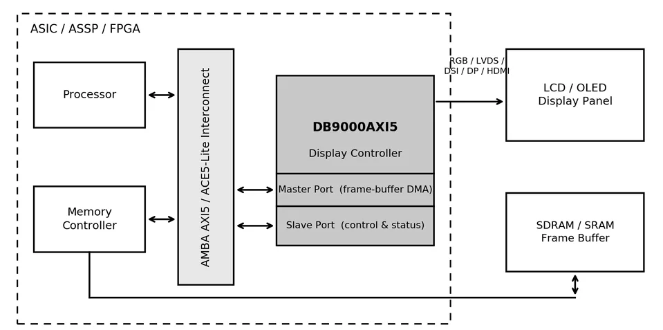
The Display Controller IP Core interfaces a microprocessor and frame buffer memory via an AMBA AXI5 / ACE5-Lite Protocol Interconnect to a TFT LCD or OLED display panel.
Overview
The Digital Blocks DB9000AXI5 Display Controller IP Core interfaces a microprocessor and frame buffer memory via an AMBA AXI5 / ACE5-Lite Protocol Interconnect to a TFT LCD or OLED display panel. It is the DB9000AXI4 core with an AXI5-capable read master: coherent, real-time and safety-ready, for SoCs whose interconnect has moved to AMBA 5.
AXI5 is defined as a set of independently negotiable interface properties rather than a single compliance level, and the DB9000AXI5 follows that model. Each property below is an independent synthesis option, licensed and built only where required; with every property disabled the DB9000AXI5 is functionally an AXI4 core, and all AXI5 registers reset such that a reset core behaves exactly as the DB9000AXI4 does today. There is no flag day for existing designs.
Key features
AXI5 Features
- ACE5-Lite I/O coherency:
- The display reads frame buffers through the coherency fabric, snooping CPU and GPU caches, and receives current data whether it is in memory or still dirty in a cache — the cache-maintenance calls in the frame buffer driver are removed and the frame buffer is allocated as normal cacheable memory
- ReadOnce and ReadOnceMakeInvalid snoop transactions (ARDOMAIN, ARSNOOP); deallocating reads for the base screen, which consumes each line exactly once per frame
- The controller has no cache of its own, so it is never snooped — no snoop address, response or data channel is added
- Guaranteed bandwidth and latency:
- MPAM partition identifier per transaction (ARMPAM), allocating the display a guaranteed share of shared-cache capacity and memory bandwidth rather than a priority hint
- Per-requester QoS (ARQOS) for base screen, overlay windows, cursor and frame descriptor fetches, plus the full AXI4 control set — ARCACHE, ARPROT, ARREGION
- Read data chunking (ARCHUNKEN, RCHUNKV, RCHUNKNUM, RCHUNKSTRB): long bursts for DRAM page efficiency with early, possibly out-of-order chunk return — shortening time-to-first-pixel at start of frame and start of line, and speeding Input FIFO recovery after a bandwidth excursion. The master falls back to strictly in-order return when the completer does not support chunking
- Functional safety:
- AXI5 check / parity signal groups across address, ID, control, data, response and handshake, generated on what the core drives and verified on what it receives; each sub-group independently enabled
- RPOISON handling — data known to be corrupt (for example an uncorrectable DRAM ECC error) is detected before it reaches the panel, rather than being displayed
- Errors are logged with the failing channel and transaction ID and raise a dedicated bus-check-error interrupt; a programmable safe-state response policy selects the deterministic behavior on a detected poison or check error
- Complements the CRC Check Per Region and Frozen Display Monitor options to form three layers of display-path integrity checking
- Protected media path:
- Non-secure Access Identity (ARNSAID) and RME security state (ARNSE) let the controller read TrustZone protected HDR and DRM video surfaces that the host CPU cannot, and composite them with unprotected graphics planes
- Wakeup, trace and wide data:
- AWAKEUP signalling so the interconnect and memory system leave low-power states deterministically ahead of a frame rather than being woken by the first transaction
- ARTRACE / RTRACE transaction tagging for system trace capture, correlating an Input FIFO underrun event with interconnect activity
- Data width parameterizable to 1024 bits
- Property-selectable: every AXI5 feature above is an independent synthesis option; all disabled equals DB9000AXI4
Display Controller Features
- Wide range of programmable display panel resolutions:
- 8K / 4K / HD high-resolution displays down to 320×240 panels; maximum programmable resolution 4096×4096 per port
- Horizontal pixel resolutions from 16 to 4096 pixels in 16-pixel increments
- Programmable 1, 2, 4 or 8-port LCD / OLED display panel interface:
- 18-bit digital (6 bits/color) and 24-bit digital (8 bits/color) parallel RGB
- Interfaces to LVDS, MIPI DSI, DisplayPort, DVI, HDMI, V-by-One and BT.656 transmitters
- Programmable frame buffer bits-per-pixel (bpp) color depths:
- 1, 2, 4, 8 bpp mapped through the Color Palette
- 16, 18, 24 bpp driving the panel directly (30 bpp with the HDR option)
- Programmable output format: RGB 6:6:6 / 5:6:5 / 5:5:5 on the 18-bit interface, RGB 8:8:8 on the 24-bit interface
- Color Palette RAM to reduce frame buffer storage and bus bandwidth:
- 256-entry × 16-bit RAM, implemented as 128 entries × 32 bits
- Loaded through the Slave Port statically by the microprocessor, or through the Master Port dynamically each frame by the DMA controller
- Programmable horizontal and vertical timing parameters — front porch, back porch, sync width, pixels-per-line, lines per-panel, and sync polarity
- Programmable pixel clock — divider from 1 to 128 of the bus clock, programmable polarity, or direct drive from an external pixel clock
- Programmable Data Enable timing signal, derived from the horizontal and vertical timing parameters, with programmable polarity
- AMBA AXI5 interconnect:
- Selectable 1024 / 512 / 256 / 128 / 64 / 32-bit AXI5 Master Port for DMA access of frame buffer memory
- Selectable AXI4-Lite (or AHB / APB) Slave Port for the control & status interface to the microprocessor
- Programmable outstanding read requests and burst lengths up to 256 beats
- 64-bit frame buffer addressing through the address-extension register
- Three memories:
- Input FIFO decoupling the bus clock from the panel pixel clock, integrated with the DMA controller
- 256-word × 16-bit Color Palette RAM
- Output FIFO
- FIFOs parameterizable in depth and width
- Linux OS frame buffer driver supplied with the core; with I/O coherency enabled the driver's cache-maintenance path is removed
- Power up and down sequencing support, with PWM backlight control
- 15 (plus the AXI5 bus-check-error interrupt) sources of internal interrupts with masking control
- Little-endian, big-endian, or Windows CE mode
- Compliance with the following specifications:
- AMBA AXI Protocol Specification — AXI5 and ACE5-Lite
- AMBA AXI4-Lite / AHB / APB for the control & status Slave Port
- Fully-synchronous, synthesizable Verilog RTL core, with rising-edge clocking, no gated clocks and no internal tri-states
Display Resolution Support — Additional Information
- Example high resolutions: Digital Cinema Systems (DCI) 2048×1080 2K and 4096×2160 4K images, and Cinema Scope HD 2560×1080.
- Example high resolutions: 7680×4320, 4096×2560, 3840×2160, 2560×2048, 2048×2048, 2048×1536, 1920×1200, 1920×1080, 1680×1050, 1600×1200, 1600×900, 1440×900, 1366×768, 1280×1024, 1280×768, 1080×1920, 1024×768, 1024×600, 1024×576, 960×540, 800×600, 800×480.
- Example medium / small resolutions: 640×480, 640×400, 640×240, 640×200, 480×800, 480×640, 480×272, 480×234, 320×240, 320×200, 240×400, 240×320, 240×240.
Block Diagram
What’s Included?
The DB9000AXI5 is available in synthesizable RTL Verilog, along with a simulation test suite, Linux driver, Synopsys Design Constraints (SDC), a simulation test bench with expected results, datasheet, and user manual.
Specifications
Identity
Files
Note: some files may require an NDA depending on provider policy.
Provider
Learn more about Digital Blocks' Display Controller IP core
Frequently asked questions about Display Controller IP
What is AMBA AXI5 / ACE5-Lite TFT LCD / OLED Display Controller?
AMBA AXI5 / ACE5-Lite TFT LCD / OLED Display Controller is a Display Controller IP core from Digital Blocks, Inc. listed on Semi IP Hub.
How should engineers evaluate this Display Controller?
Engineers should review the overview, key features, supported foundries and nodes, maturity, deliverables, and provider information before shortlisting this Display Controller IP.
Can this semiconductor IP be compared with similar products?
Yes. Buyers can compare this product with similar semiconductor IP cores or IP families based on category, provider, process options, and structured technical specifications.