ITP-STDP: An Intrinsic-Timing Power-of-Two Learning Engine for On-Chip SNN Training
By Haihang Xia 1, Xinyu Zhao 1, Xuecheng Wang 1, John Goodenough 1, Charith Abhayaratne 1, Panagiotis A. Panagiotou 1, Chunyi Song 2,3,4, and Tiantai Deng 5
1 School of Electrical and Electronic Engineering, The University of Sheffield, U.K.
2 Donghai Laboratory, Zhoushan 316021, China
3 Engineering Research Center of Oceanic Sensing Technology and Equipment, Ministry of Education, Zhoushan 316021, China
4 State Key Laboratory of Ocean Sensing and Ocean College, Zhejiang University, Zhoushan 316021, China.
5 Donghai Laboratory, Zhoushan 316021, China
Abstract
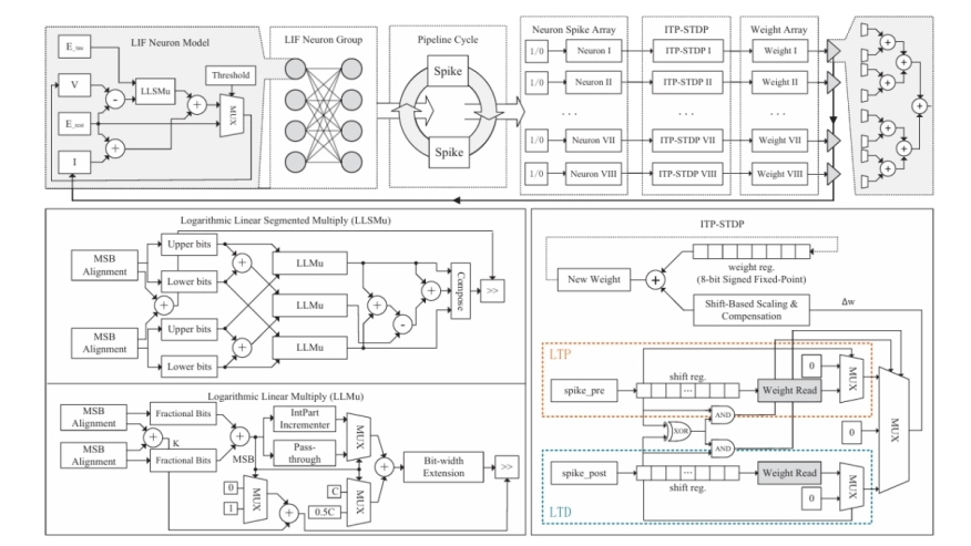
Spiking neural networks (SNNs) have the potential to emerge as the third generation of neural networks and have attracted increasing attention across a wide range of applications. However, the large number of synaptic connections in SNNs leads to intensive weight-update computation by on-chip learning algorithms during training, resulting in substantial hardware resource utilization and energy consumption. Among existing SNN learning algorithms, spike-timing-dependent plasticity (STDP) is one of the most extensively studied and widely adopted, serving as a fundamental learning component in SNNs. To address the hardware and energy overheads associated with SNN training, this paper presents intrinsic-timing power-of-two STDP (ITP-STDP) and its corresponding prototype learning engine hardware architecture. The proposed design is evaluated through a dedicated mean-field synaptic drift model for dynamical analysis and further validated across SNN networks of different scales and datasets. It is further implemented on both ASIC and FPGA platforms and compared with state-of-the-art approaches, including the original STDP and more complex STDP variants. The results demonstrate superior energy efficiency, higher operating speed, and substantially lower hardware resource utilization, as the proposed design eliminates most of the computational overhead of STDP through both algorithmic and hardware-level optimizations. On the FPGA platform, the proposed design improves energy efficiency by 4.5x to 219.8x over the compared designs. On the ASIC platform, the proposed design achieves a 4.8x to 22.01x speedup while consuming only 1.2% to 3.3% of the area required by prior works.
To read the full article, click here
Related Semiconductor IP
- Adaptive Voltage Scaling (AVS) Bus Target IP
- Adaptive Voltage Scaling (AVS) Bus Host Controller
- NoC Interconnect IP Generator
- Over-Voltage Lockout (OVLO) IP
- Verification IP for Universal Chiplet Interconnect Express (UCIe) up to 3.0
Related Articles
- Display Driver with on-chip frame buffer and a scalable image compression engine
- Aircraft Jet Engine Failure Analytics Using Google Cloud Platform Based Deep Learning
- All-in-One Analog AI Hardware: On-Chip Training and Inference with Conductive-Metal-Oxide/HfOx ReRAM Devices
- relOBI: A Reliable Low-latency Interconnect for Tightly-Coupled On-chip Communication
Latest Articles
- Low-Energy Reduced RISC-V Instruction Subset Processor for Tsetlin Machine Inference at the Edge
- Si-GT: Fast Interconnect Signal Integrity Analysis For Integrated Circuit Design Via Graph Transformers
- Hardware Mechanisms to Dynamically Throttle AI Performance
- SEAM-V: A Hybrid-Decoupled RISC-V Vector Processor with Backend-Visible EP Context for Sustained Vector Throughput
- New Number Formats for FFT IP Cores in Optical OFDM Transceivers