Tape-Out Readiness Checklist: Engineering Decisions That Prevent Costly Respins

Tape-out is the moment when an ASIC design moves from being a plan to becoming a real chip. At this stage, functional behaviour, timing, power, physical layout, testability, and manufacturability must all be well understood and verified.
 A design might work correctly on paper but still fail in practice due to issues such as clock domain crossings (CDC), incorrect timing rules, voltage drops (IR), electromigration (EM), routing problems, or problems that arise during manufacturing.
Fixing these after tape-out is very costly.
A strong tape-out process should fix problems step by step, not just check things once at the end before releasing the final design files (GDSII).
Phase 1: Front-End Architecture and RTL Sign-Off
RTL Linting, CDC, and RDC Verification
Issues like unintended latches, signals from multiple sources, incomplete assignments, crossings between clock domains, and crossings between reset domains can go undetected until the chip is made.
Formal checks for CDC and RDC should make sure that the behavior of asynchronous signals and resets is correct. Special attention is needed for situations that could cause unstable signals, reset order, and how synchronizers are used.
Any exceptions should be checked and recorded before finalizing the RTL design.
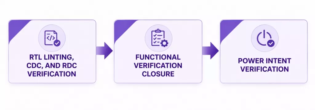
Figure 1: Front-End Architecture and RTL Sign-Off
Functional Verification Closure
Functional testing should cover both normal operation and rare situations that are hard to reach with simulation.
Using constrained-random UVM tests gives a wide range of inputs, while formal verification helps prove correct behavior in parts of the design that are controlled, like arbiters, decoders, state machines, and protocol managers.
Testing should cover all parts of the code, like statements, branches, changes, and state machines, as well as functional coverage.
The goal is not just to reach a high percentage, but to understand why some parts are not covered. Every missing part should have a reason and be checked by others.
Power Intent Verification
Features like multiple voltage levels, power gates, isolation cells, level shifters, and power-saving elements must work together across different power modes.
The power intent language (UPF or CPF) should match the RTL and the final design.
Testing should check how the chip behaves during power-up, power-down, isolation, retention, and wake-up steps to make sure everything works properly when changing power modes.
Phase 2: Synthesis and Netlist Sign-Off
SDC Constraint Validation
Missing clocks, wrong definitions for generated clocks, false paths, paths that take more than one cycle, and inputs that are not constrained can result in incorrect timing analysis.
SDC constraints should be checked for correct syntax, completeness, consistency, and proper intent.
Relationships between clocks should be clearly defined, not left for the tool to guess. Every timing exception should have a clear reason and be reviewed as part of timing sign-off.

Figure 2: Synthesis and Netlist Sign-Off
Phase 3: Physical Implementation and P&R
DFT Implementation and Physical Optimization
DFT structures such as scan chains, MBIST, boundary scan, compression logic, and test clocks affect area, timing, routing, and power. Their implementation therefore needs to be considered alongside physical design rather than treated as an isolated pre-layout activity.
Scan chains should be planned with placement, power domains, clocking, and routing in mind. Physically aware scan-chain reordering can help reduce routing overhead and avoid unnecessary crossings between power domains. Test-mode switching activity should also be analysed to manage peak power during scan shift and capture.

Figure 3: Physical Implementation and P&R
Floorplanning and Power Network Synthesis
Large memory blocks, fixed IPs, PHYs, and other big components can cause problems if placed without thinking about nearby routing and power needs.
Early global routing and power analysis can help find these problems before detailed layout is done.
Routing and power margins should be based on the technology, block density, macro placement, and expected activity, not just a fixed percentage for all designs.
Blocks with high current should be placed in a way that considers the power grid and how voltage drops might happen.
Clock Tree Synthesis
Clock Tree Synthesis (CTS) using MCMM should optimize for skew, delay, transition, clock uncertainty, and clock power.
Clock routing should also consider signal coupling and electromigration.
The way you build the clock structure depends on how the clock is organized, the layout of the chip, the technology used to make it, and the timing needs.
Phase 4: Full-Chip Sign-Off
Timing, IR Drop and Electromigration Sign-Off
Even if a design passes static timing analysis, it might still fail in real silicon due to voltage drops or reliability issues.
It should also look at extracted parasitic effects, both static and dynamic IR drop, electromigration, and signal integrity if needed.
Timing margins, voltage variations, clock behavior, and reliability limits all need to be checked together under real conditions.
The space between the design and the final product should reflect the specific needs of the technology and the product, not just some fixed number everyone uses.
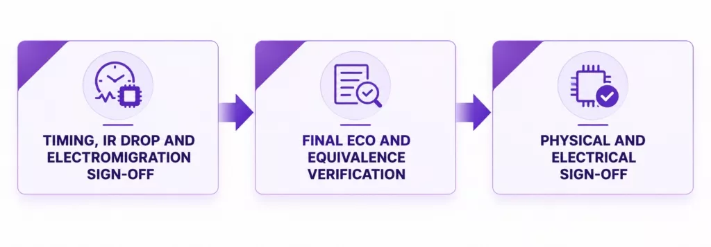
Figure 4: Full-Chip Sign-Off
Final ECO and Equivalence Verification
Sometimes, changes to the design occur late, especially when timing or physical issues arise.
After major changes, it is important to check that the design is still the same as the original using formal equivalence or some logical comparison method.
Also, timing, design for test, physical checks, and power integrity should be rechecked if the change might affect them.
The final version of the design database should match the approved version and show the full history of all the changes made.
Physical and Electrical Sign-Off
At smaller manufacturing processes, checking the physical layout goes beyond just checking for basic design rule violations.
With very dense layouts, there are new issues to worry about, like antenna effects, metal density, pattern-specific rules, and other foundry-specific guidelines.
During the design process, using a hierarchical approach to check for design rule compliance, layout versus schematic, and electrical rule checks helps find problems before they become big issues.
The final sign-off should use the most up-to-date and approved rules from the foundry, applied to the exact database that will be released.
Each decision to ignore a rule should be approved and documented, not just carried forward without reason.
Phase 5: Production and Data Release
ATPG and Tester Vector Handoff
The patterns need to work with the final gate-level design and the environment the test equipment will use.
The patterns should be tested using the correct fault models and, when needed, simulated with gate-level timing information.
Formats like STIL or WGL should be checked before they are handed over.
Test coverage should match the product’s quality goals and test plan, not just aim for a standard percentage.
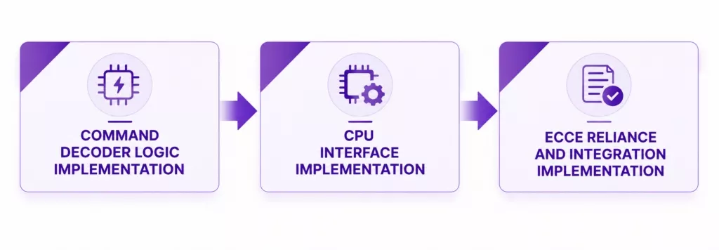
Figure 5: Production and Data Release
DFM and Yield Optimization
Problems like lithography, vias, density, and layout patterns can all affect how many chips work.
DFM checks should cover the specific issues related to the manufacturing process, including critical area analysis, via redundancy, density analysis, and pattern hotspot detection.
Techniques like adding extra vias to improve yield should be used when they are supported and justified.
GDSII Release and Mask Data Preparation
Layer mapping, hierarchy, IP versions, metal fill, seal structures, test structures, and other manufacturing data must all match the approved release configuration.
The final GDSII file should be created in a controlled, isolated environment.
The data should then be checked independently before it is sent to the foundry.
To make sure the files are correct, use modern cryptographic hashes like SHA-256, not just MD5.
Tape-Out Is the Final Risk-Closure Decision
It is the result of combining many checks: functional correctness, timing, power, physical checks, testability, manufacturability, and data consistency.
The final question is simple:
Is the exact database being released functionally correct, timing clean, physically verified, power safe, testable, manufacturable, and traceable back to the original approved design?
If the answer still depends on a guess, an unexplained exception, or a change that was not properly checked, the design is not ready for tape-out.
The purpose of having a clear checklist for tape-out is to find expensive problems before they become too costly to fix.
To get ready for tape-out, you need to do everything right across a few areas: RTL, verification, physical implementation, DFT, and final sign-off.
As a partner of TSMC DCA and in collaboration with various other foundries, MosChip works with the foundry to help customers with the process of developing silicon through tape-out with first-pass success.
MosChip brings expertise Silicon design expertise spanning RTL design and verification, synthesis, DFT, physical design, and turnkey ASIC execution for analog and mixed-signal design. This helps silicon teams address design risks early and maintain consistency through sign-off and final data release.
Related Semiconductor IP
- NPU IP
- JPEG XL Encoder
- I2C Master/Slave Controller Core
- NVMe Validation Test Suite
- Hybrid Memory Cube Verification IP
Related Blogs
- TSMC To Tape-Out 20nm Apple Processor This Month
- MIPI UniPro: Comprehensive Verification Checklist
- The Risks & Rewards of Early Tapeout
- Synopsys Accelerates Multi-Die System Designs With Successful UCIe PHY IP Tape-Out on TSMC N3E Process
Latest Blogs
- Tape-Out Readiness Checklist: Engineering Decisions That Prevent Costly Respins
- How Cadence DSPs Put In-Cabin AI Audio On-Chip in SemiDrive's X10
- The Fastest Path to Scalable Photonic Systems: Using Proven IP for both PIC and EIC designs
- Building Trusted AI Agents from the Silicon Root of Trust
- Heterogeneous Computing in Space