Samsung Foundry and Cadence Expand Infrastructure and Physical AI Solution

Today, AI infrastructure is driving a fundamental shift in semiconductor design. Delivering the next generation of AI systems requires more than advanced process technology; it demands seamless integration across chiplets, 3D-ICs, advanced packaging, high-bandwidth interconnects, memory, and system optimization. As the industry moves toward sub-2nm and physical AI expands beyond the data center, managing system-level complexity is becoming a critical differentiator.
 That broader transition sits at the center of Cadence's expanded collaboration with Samsung Foundry around their third-generation GAA process technology.
The multi-year agreement builds on the companies' existing collaboration and expands Cadence's role in enabling AI-scale semiconductor development on Samsung Foundry's second-generation 2nm platform. By broadening its advanced Memory and Interface IP portfolio—including PCIe 7.0, UCIe 64G, HBM5, 224G/256G SerDes, and NVIDIA NVLink-C2C-enabled interconnect—and extending its agentic AI-driven digital, custom, 3D-IC, and system design and analysis (SDA) flows, Cadence is helping create a signoff-ready platform for developing next-generation infrastructure AI and physical AI systems.
Infrastructure AI Is Reshaping Advanced-Node Design Requirements
Modern AI systems rely on high-bandwidth memory, heterogeneous compute, advanced interconnect fabrics, and multi-die integration, reshaping priorities at leading-edge process nodes.
Performance-per-watt, interconnect efficiency, packaging scalability, and design convergence are becoming just as important as transistor density itself. Samsung Foundry's 2nm process is designed to address these demands, but delivering AI-scale systems also requires closer coordination across implementation, packaging, verification, and signoff workflows.
This new multi-year agreement further broadens the Cadence portfolio of Memory and Interface IP available across Samsung Foundry's advanced process technologies, including:
- GDDR7 memory for advanced computing, including graphics rendering, simulations
- DDR5 MIDIMM 12.8G combo solutions optimized for high-bandwidth memory subsystems
- LPDDR6/LPDDR5X memory interface IP for performance- and power-sensitive AI systems
- HBM5 IP support for next-generation AI accelerator memory bandwidth scaling
- PCIe 7.0 IP for next-generation high-bandwidth accelerator and system connectivity
- PCIe 6.0 IP for advanced AI and HPC platforms
- NVIDIA NVLink-C2C-enabled interconnect IP for high-speed chip-to-chip communication
- UCIe Standard Package (UCIe-S) 64G and UCIe Advanced Package (UCIe-A) 64G IP for chiplet-based integration
- 224G/256G high-speed SerDes and PCIe combo IP for AI fabric and hyperscale interconnect requirements
- 10G MP-PHY IP for advanced die-to-die and multi-protocol connectivity
Explore Cadence IP:
Enabling a Production-Ready AI Development Ecosystem
The demand for compute and AI capabilities for data centers and AI factories is driving the need to quickly expand AI infrastructure. As members of the NVIDIA NVLink Fusion ecosystem, Cadence and Samsung are working together to provide NVLink-C2C-enabled interconnect IP for Samsung's 2nm process.
The collaboration also extends support for NVIDIA CUDA-X GPU-accelerated libraries, allowing Cadence's implementation, analysis, and signoff solutions to run key workloads on the Cadence Millennium Supercomputers, built on NVIDIA GPU/CPU compute platforms. Combined with deeper enablement of Cadence's certified AI-driven implementation and signoff flows enabled on Samsung Foundry, this helps engineering teams accelerate design convergence while developing increasingly complex AI, HPC, and 3D-IC systems.
Together, these capabilities address key scaling challenges in modern AI system, enabling scale-up and scale-out architectures. PCIe 7.0, NVLink-C2C, UCIe, HBM5, and 224G/256G SerDes are not incremental interface upgrades; they are foundational technologies for scaling chiplet architectures, AI fabrics, memory bandwidth, and heterogeneous computing accelerator systems. More importantly, the collaboration is creating a production-ready development environment that brings IP, implementation, packaging, verification, and signoff into a more integrated engineering workflow.
Cadence Is Building a More Integrated AI System Design Platform
Traditional EDA workflows become increasingly difficult to sustain as AI systems move toward chiplet architectures and 3D integration. AI-era semiconductor systems are now engineered as interconnected platforms spanning chiplets, memory stacks, interconnect fabrics, advanced packaging, and heterogeneous compute domains that must converge simultaneously across power, thermal, timing, reliability, and manufacturability constraints.
To address these challenges, Cadence has expanded its certified AI-driven implementation and signoff platform for Samsung Foundry's SF2P node across digital, custom, 3D-IC, analysis, signoff, and verification flows. The certified flow includes:
- Innovus Implementation System for digital implementation
- Virtuoso Studio for analog and custom design
- Integrity 3D-IC Platform for full 3D-IC system planning and implementation
- Voltus IC Power Integrity Solution for power integrity and system-level power analysis
- Quantus Extraction Solution for extraction and Tempus Timing Solution for signoff
- Pegasus Verification System for verification
- Cadence Cerebrus Intelligent Chip Explorer for intelligent design exploration and optimization
Cadence also enables key design features, including glitch power optimization within the Innovus and Genus Synthesis Solution flows, along with smart hierarchical optimization designed to improve performance, power, and area (PPA), and turnaround time (TAT).
The collaboration further extends into Samsung's Cube-H, a next-generation approach using hybrid copper bonding (HCB). The 3D-IC flow includes silicon interposer auto-routing and optimization capabilities tightly connected with implementation, analysis, and signoff technologies.
The broader significance of the collaboration is the emergence of "one-Samsung," a more tightly integrated AI system development stack where interconnect, memory, packaging, implementation, verification, and AI-assisted optimization are engineered together rather than as isolated domains.
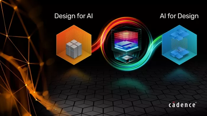
Where Design for AI and AI for Design Intersect
Cadence and Samsung Foundry are enabling more complex infrastructure AI and physical AI systems on 2nm, while using AI-assisted implementation and GPU-accelerated workflows to accelerate design, verification, and tapeout.
That shift fundamentally changes the role of EDA. As AI SoCs and chiplet-based systems grow in scale, engineering productivity itself is becoming a strategic bottleneck. At advanced nodes, every additional design iteration incurs a significant cost, making a faster confluence of workflow automation economically critical. Advanced-node implementation now involves multidimensional optimization spanning timing closure, power integrity, thermal behavior, reliability, and package interaction.
Cadence's expanded enablement reflects the growing role of agentic AI and GPU acceleration in advanced-node development. The company's agentic AI implementation capabilities, hierarchical optimization flows, and GPU-accelerated design infrastructure are designed not only to improve PPA but also to reduce iteration cycles, accelerate design convergence, automate workflow optimization, and shorten time to tapeout as infrastructure AI platforms continue growing in complexity.
So, who's embracing these joint solutions?
NVIDIA: The Growing Importance of AI Interconnect Infrastructure
NVIDIA is leveraging Cadence's GPU-accelerated flows and NVLink-C2C-enabled infrastructure on Samsung Foundry's 2nm platform to optimize next-generation accelerated computing architectures and high-bandwidth interconnect technologies.
As AI clusters continue to scale, efficient chip-to-chip communication is becoming a defining constraint on system performance. NVLink-C2C plays a critical role in enabling the tightly coupled heterogeneous compute architectures and high-speed chiplet communication required for large-scale AI infrastructure.
"As AI workloads scale and system architectures grow more demanding, the semiconductor ecosystem depends on tools and platforms that can keep pace with simulation and design complexity at advanced nodes. By leveraging Cadence's GPU-accelerated design flows on Samsung Foundry's second-generation 2nm platform, we're optimizing the performance and delivery of next-generation AI architectures and high-bandwidth interconnects."
- Timothy Costa, vice president and general manager of computational engineering, NVIDIA.
Ambarella: Physical AI Is Expanding Advanced Compute Beyond the Data Center
Ambarella's next-generation 2nm edge AI platform demonstrates how Cadence's signoff-ready IP, implementation flows, and system analysis technologies are supporting robotics, drones, autonomous machines, and intelligent sensing platforms that require high-performance AI acceleration within highly constrained power and thermal envelopes.
Physical AI systems pose a very different design challenge than cloud-scale AI accelerators. These systems must combine AI compute, sensor fusion, real-time responsiveness, low-power operation, and highly reliable system behavior within compact edge environments. That significantly increases the importance of co-optimized implementation, verification, and signoff workflows at advanced nodes.
According to Ambarella COO Chan Lee, Cadence's PCIe-based connectivity solutions on Samsung's advanced 2nm process node, combined with signoff-ready flows and co-optimized design tools, have been instrumental in helping the company manage the complexity of next-generation edge AI development.
"Having a signoff-ready, co-optimized IP and tools solution, together with a robust, production-proven design kit and PDK, enables our teams to move forward with confidence, reduce risk, and stay focused on accelerating innovation in low-power AI perception, physical AI, and intelligent edge computing."
- Chan Lee, COO, Ambarella
Reducing Complexity Across the AI System Design Stack with the Cadence – Samsung Foundry Co-Optimized Platform
The broader significance of the Cadence-Samsung Foundry collaboration is that it reflects how semiconductor development itself is evolving in the AI era.
Advanced-node leadership is no longer defined solely by transistor scaling. It is increasingly defined by the ability to deliver integrated ecosystems spanning IP, implementation, packaging, interconnect, verification, signoff, GPU acceleration, and AI-assisted optimization. Companies that can reduce friction across the AI system design stack—from architecture exploration through implementation and signoff—will be best positioned to accelerate the next generation of infrastructure AI and physical AI systems.
Learn more about the expanded Cadence-Samsung Foundry collaboration and its role in accelerating next-generation infrastructure AI and physical AI development on Samsung Foundry's second-generation 2nm process.
Related Semiconductor IP
- 224G-LR SerDes PHY
- Highly scalable performance for classic and generative on-device and edge AI solutions
- MIPI CSI-2 TX Controller
- 1.6T Ultra Ethernet Controller
- HBM4E PHY and controller
Related Blogs
- Cadence Silicon Success of UCIe IP on Samsung Foundry’s 5nm Automotive Process
- Rethinking AI Infrastructure: The Rise of PCIe Switches
- Securing Scale-Up AI: Cadence’s Complete UALink Solution
- DDR5 MRDIMM Gen2: The Missing Link in Scaling AI Infrastructure
Latest Blogs
- Tape-Out Readiness Checklist: Engineering Decisions That Prevent Costly Respins
- How Cadence DSPs Put In-Cabin AI Audio On-Chip in SemiDrive's X10
- The Fastest Path to Scalable Photonic Systems: Using Proven IP for both PIC and EIC designs
- Building Trusted AI Agents from the Silicon Root of Trust
- Heterogeneous Computing in Space