Highly scalable performance for classic and generative on-device and edge AI solutions
Scalable and Power-Efficient Neural Processing Units The Neo NPUs offer energy-efficient hardware-based AI engines that can be pa…
Overview
Scalable and Power-Efficient Neural Processing Units
The Neo NPUs offer energy-efficient hardware-based AI engines that can be paired with any host processor for offloading artificial intelligence and machine learning (AI/ML) processing. The Neo NPUs target a wide variety of applications, including sensor, audio, voice/speech, vision, radar, and more. The comprehensive performance range makes the Neo NPUs well-suited for ultra-power-sensitive applications such as IoT, hearables/wearables, high-performance systems in AR/VR, automotive, and more.
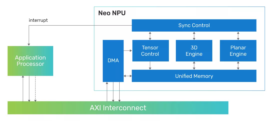
The product architecture natively supports the processing required for many network topologies and operators, allowing for a complete or near-complete offload from the host processor. Depending on the application’s needs, the host processor can be an application processor, a general-purpose MCU, or a DSP for pre-/post-processing and associated signal processing, with the inferencing managed by the NPU.
The Neo NPUs provide performance scalability from 256 up to 32k 8x8-bit MAC per cycle with a single core, suiting an extensive range of processing needs. Capacity configurations are available in power-2 increments, allowing for the right sizing in an SoC for the target applications. Int4, Int8, Int16, and FP16 are all natively supported data types, with mixed precision supported by the hardware and associated software tools, allowing for the best performance and accuracy tradeoffs.
Additional features of the Neo NPUs include compression/decompression to minimize system memory space and bandwidth consumption for a network and energy-optimized compute hardware to leverage network sparsity tradeoffs.
The Neo NPUs support typical clock frequencies of up to 1.25GHz in 7nm, and customers can target lower clock frequencies for specific product needs.
Key features
- Single-core performance up to 80 TOPS
- Configurable range of 256 MACs per cycle to 32k MACs per cycle
- Upward-scalable with multi-core topologies for 100s of TOPS
- Efficient offload and execution of neural network processing from any application host processor
- Built-in support for many networks, including CNN, RNN, Transformer, and more
- Built-in support for multiple data types, including int4, int8, int16, and fp16
- Application targets varied across many domains (sensor, audio, vision, radar) and markets (IoT, hearables/wearables, AR/VR, automotive)
Block Diagram
Benefits
- Single-core performance up to 80 TOPS
- Configurable range of 256 MACs per cycle to 32k MACs per cycle
- Upward-scalable with multi-core topologies for 100s of TOPS
- Efficient offload and execution of neural network processing from any application host processor
- Built-in support for many networks, including CNN, RNN, Transformer, and more
- Built-in support for multiple data types, including int4, int8, int16, and fp16
- Application targets varied across many domains (sensor, audio, vision, radar) and markets (IoT, hearables/wearables, AR/VR, automotive)
What’s Included?
- Free Software Evaluation
- Try our SDK Software Development Toolkit for 15 days absolutely free. We want to show you how easy it is to use our Eclipse-based IDE.
- Online Support
- The Cadence Online Support (COS) system fields our entire library of accessible materials for self-study and step-by-step instruction.
- Xtensa Processor Generator (XPG)
- The Xtensa Processor Generator (XPG) is the heart of our technology - the patented cloud-based system that creates your correct-by-construction processor and all associated software, models, etc. (Login Required)
- Technical Forums
- Find community on the technical forums to discuss and elaborate on your design ideas.
Specifications
Identity
Files
Note: some files may require an NDA depending on provider policy.
Provider
Learn more about Edge AI Accelerator IP core
Dream Chip, Cadence Unveil Automotive SoC with Tensilica IP at embedded world '25
Tensilica at CES
Beyond PCIe Compliance: Why Stress Testing Is Crucial for Edge AI Deployments
Rethinking Edge AI Interconnects: Why Multi-Protocol Is the New Standard
One PHY, Zero Tradeoffs: Multi-Protocol PHY for Edge AI Interface Consolidation
Frequently asked questions about Edge AI Accelerator IP cores
What is Highly scalable performance for classic and generative on-device and edge AI solutions?
Highly scalable performance for classic and generative on-device and edge AI solutions is a Edge AI Accelerator IP core from Cadence Design Systems, Inc. listed on Semi IP Hub.
How should engineers evaluate this Edge AI Accelerator?
Engineers should review the overview, key features, supported foundries and nodes, maturity, deliverables, and provider information before shortlisting this Edge AI Accelerator IP.
Can this semiconductor IP be compared with similar products?
Yes. Buyers can compare this product with similar semiconductor IP cores or IP families based on category, provider, process options, and structured technical specifications.