Cadence Demonstrates PCIe 8.0 PHY at PCI-SIG DevCon 2026
The accelerated growth in data processing and storage demands across HPC data centers and AI factories is expediting PCIe innovation as PCIe links form a foundational fabric for xPU and storage connectivity.
While PCIe 6.x is now being deployed in AI factories and HPC datacenters, PCIe 7.0 is advancing through product and platform development. At the same time, work on PCIe 8.0 PHY is already underway, even though the specification is at least a year from being final.
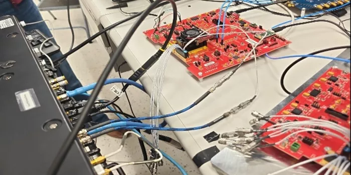
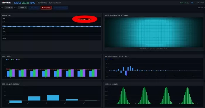
PCIe 8.0 once again follows the cadence of doubling the IO speed, taking us to 256 GT/s, pushing SerDes and PHY design into highly challenging territory. Achieving this leap requires tightly coupled optimization across performance, power, and area. Demonstrating its leadership in high-speed connectivity, Cadence successfully showcased a PCIe 8.0-capable SerDes at PCI-SIG DevCon US (May 6–7, 2026) at the Santa Clara Convention Center.
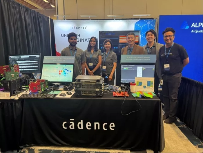
In the demonstration, a data link was established using a Keysight arbitrary waveform generator (AWG) transmitting to a Cadence PHY receiver. The system demonstrated good bit error rate (BER) performance. The SerDes used in the demo builds on Cadence's advanced DSP-based transceiver architecture, which has been leveraged across multiple generations of PAM4-based standards, including PCIe 64 GT/s and 128 GT/s, as well as Ethernet 56G, 112G, and 224G.
PCIe 8.0 continues the industry's push toward higher bandwidth, delivering up to 1 TB/s of bidirectional throughput in a x16 configuration. It serves as a scalable interconnect solution for emerging applications in AI/ML, HPC, networking, and storage. The standard builds on key innovations introduced in PCIe 6.x and 7.0, including PAM4 signaling, FLIT-based encoding, forward error correction (FEC), and the L0P low-power state for dynamic bandwidth scaling and energy efficiency. Additional features such as link-level retry, multipath I/O, peer-to-peer and UIO for low-latency data transfer, enhanced security (CMA/IDE), and virtualization support (SR-IOV/SIOV) further strengthen its capabilities.
Looking ahead, PCIe 8.0 also extends reach with advanced electrical and optical retimers, enabling connectivity within and beyond the rack, which is becoming essential for disaggregated AI infrastructure and scale-up/scale-out architectures.
Cadence remains a leading provider of PCIe PHY and controller IP. From the early days of the PCIe standard, Cadence solutions have been widely adopted across datacenter, enterprise, consumer, automotive, and networking applications. As the PCIe ecosystem evolves, Cadence continues to play a key role in enabling next-generation interconnect solutions for AI/ML, xPU, storage, and HPC systems.
Learn more about Cadence PCIe offerings: PHY for PCIe and CXL.
Related Semiconductor IP
- PCIe 5.0 Serdes PHY IP, Silicon Proven in TSMC 16FFC
- PCIe 3.1 Serdes PHY IP, Silicon Proven in TSMC 40LP
- PCIe 3.1 Serdes PHY IP, Silicon Proven in TSMC 28HPCP
- PCIe 6.0 / CXL 3.0 PHY & Controller
- Simulation VIP for PIPE PHY
Related Blogs
- Cadence Leads the Way at PCI-SIG DevCon 2025 with Groundbreaking PCIe 7.0 Demos
- Video: Cadence Demonstrates PCIe Gen3 Silicon at PCI-SIG Dev-Con (SAS RAID Controller)
- Cadence Demonstrates Complete PCIe 7.0 Solution at PCI-SIG DevCon 24
- Cadence support for the Open NAND Flash Interface (ONFI) 3.0 controller and PHY IP solution + PCIe Controller IP opening the door for NVM Express support
Latest Blogs
- World's First Standards-Compliant 112G PHY IP for Linear Optics: A Turning Point for AI Interconnects
- One Key for Every Door: How Aliro Extends the UWB Digital Key Beyond the Car
- Reprogrammable Post-Quantum Security for SoCs: Why Crypto-Agility Matters
- Designing the Beam Steering Core for a C-Band AESA: A Look at VSI's VBF0644 GaAs Beamformer IC
- Secure Boot for embedded systems: Building a complete chain of trust