Leading-edge AI IC designs demand comprehensive HAV methodologies

Driven by insatiable demand to enable AI to process more data faster, the design teams building today’s most advanced ICs at the heart of AI systems rely on hardware-assisted verification to develop SoCs, software that to runs on these SoC, and finally the ability to perform full system verification and validation. Emulation, the more traditional and hardware verification focused technology in HAV, facilitates the creation of models of a given IC design in register transfer level (RTL) RTL code. This executable model gives design teams full observability into the functionality of their design and allows them to debug the IC design, make necessary corrections, and ultimately verify the design functions to its specification before sending it to layout and manufacturing, where it will become an IC.
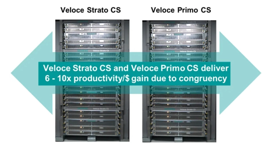 A more recent HAV technology, called FPGA-based prototyping, is trading off some hardware observability of emulation for greater execution speed. Because of its 5X to 10X increased performance over emulation, an FPGA prototyping enables software teams to develop firmware and even apps and perform system validation with software running on the hardware design before the IC design is available in silicon. They can then fix the IC design to optimize software and system performance. Having the design running on hardware also enables software teams to get an early jump on application software development. Together emulation and FPGA-based prototyping are invaluable to helping companies develop more reliable products faster. This is especially important in the AI era.
Let’s take a closer look at some HAV methodologies used for today’s most advanced AI designs.
To read the full article, click here
Related Semiconductor IP
- UALink 200G v1.0 Verification IP
- CCSDS SCCC Demapper and Turbo Decoder
- NPU IP
- JPEG XL Encoder
- I2C Master/Slave Controller Core
Related Blogs
- FD-SOI Can Deliver Leading-Edge European IC Process Technology
- Accelerating PCIe Gen6 L0p Verification for AI & HPC Designs using Synopsys VIP
- Cadence Adds 10 New VIP to Strengthen Verification IP Portfolio for AI Designs
- AI workloads demand smarter SoC interconnect design