Automatic Generation of a Network-on-Chip Interconnect

As the art of chip design began to mature, interconnecting major blocks required more than just ad hoc collections of signals. This led to the definition of on-chip buses, most notably the AMBA family developed by Arm®, to connect processors, peripherals, memory controllers, and other functions. In recent years, as system-on-chip (SoC) devices have grown even larger and more complex, there has been a corresponding evolution for interconnects. This post discusses the network-on-chip (NoC) approach and explains how Agnisys can help you generate NoCs automatically for your designs.
The Limitations of Traditional On-Chip Buses
There is no doubt that on-chip buses were a major improvement over point-to-point signal connections between functional blocks. Sharing a common bus reduced the number of connections on each interconnected unit, as well as the number of signals to be routed on the chip. The same proven bus interface design could be used for every block on the bus, reducing development time and making verification simpler. Bus families such as AMBA offered different options, typically a high-speed processor bus and a low-speed peripheral bus, to provide flexibility for your designers.
For all their benefits, traditional buses have several limitations. Although they reduce the number of signals to be routed, the bus signals tend to be long wires that traverse much of the chip. This causes congestion issues with placement of the functional blocks and routing of these signals. Scalability is also an issue, since there are typically limits on how many blocks can be connected to each bus. Finally, although some buses support pipelining, fundamentally there is only one transaction active on an on-chip bus at any point in time. This limits parallelism and thus overall throughout.
The Emergence of NoCs
In the early 2000s, academicians began to argue for on-chip packet-switched communication over point-to-point wires rather than traditional buses. As this concept was developed, the NoC term was introduced and commercial solutions began appearing 20 years ago. NoCs were designed to address the limitations of on-chip buses. Point-to-point interconnects within the network avoid the congestion problems of long global bus wires. A standard NoC interface on all blocks has all the reuse advantages of buses, and a structured architecture eliminates point-to-point connections between design blocks.
This same architecture makes NoCs much more scalable than buses. Hundreds of blocks can be interconnected without adding any new interfaces. The point-to-point connections happen between the functional units and the NoC blocks. This minimizes redesign if you add more functionality, such as additional CPUs or new I/O ports, to your chip. In addition, different transactions can happen in parallel on different paths through the chip. This provides a major boost for throughout and overall performance, making your chip more competitive in your target markets.
Structure of the NoC Design
The diagram below shows a scalable NxM NoC architecture. Blocks are interconnected across N rows and M columns, with routers at each intersection. Transactions are initiated by processing elements such as CPUs, GPUs, other engines and accelerators, and DMA units. The Ingress Network Interface (IG NI) packetizes transactions on each point-to-point AMBA AXI bus into flow control units (flits) that are routed through paths in the fabric to the Egress Network Interface (EG NI). Different types of flits are used to send data and to control the overall transaction.
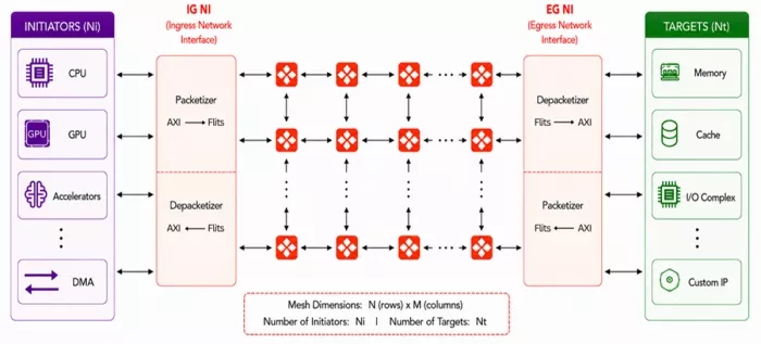
The EG NI depacketizes the flits and assembles AXI transactions that are sent to target blocks such as memory and I/O ports. Of course, most transactions are bidirectional since read data and status information must be sent back to the initiators. Thus, the EG NI is also capable of packeting return information, which is also sent through the routers, and the IG NI depacketizes it. Multiple transactions can have control and data packets flowing in both directions through the network fabric at the same time. To increase throughput, you can simply add more routers to the NoC.
Explore Agnisys IP:
Introducing IDS-NoC
Our users have relied on us for years to automatically add bus interfaces to the control and status register (CSR) and memory blocks we generate in our IDesignSpec™ Suite specification automation solution. We also interconnect these blocks as well as your custom blocks with IDS-Integrate™, including adding bus decoders, multiplexers, aggregators, bridges, and crossbar interconnects automatically when we generate the top level of your SoC. We have extended this concept with our recently announced new product IDS-NoC™.
IDS-NoC is a scalable NoC interconnect IP generation solution for modern heterogeneous multi-core SoCs. Built on a packet-switched, distributed architecture, IDS-NoC enables your designers to rapidly create, configure, and integrate high-performance interconnect fabrics. To add more endpoints (initiators and targets) or routers, you simply change the parameters and generate a new design. Our solution is compatible with Arm and RISC-V® processor-based systems and supports the development of complex, data-intensive SoCs.
The fabric designs that we generate are in unencrypted, fully portable SystemVerilog RTL. They have all the routability, scalability, and performance advantages inherent in the NoC approach. In addition:
- We have a pipelined, virtual channel architecture that eliminates structural deadlocks
- We can re-order memory transactions to improve overall system performance
- We support up to 1024 pending transactions and data bus widths of up to 2048 bits
- We offer you optional features for reliability and functional safety
- We provide parameterization at generation time, elaboration time, and run time
- We have no limits on the number of NoCs or Ni units in your design
Conclusion
NoCs have become a vital interconnection option for today’s huge SoCs for applications such as AI, data centers, automotive, and networking. By choosing IDS-NoC, you have a scalable solution that you can simply re-run anytime that your requirements change. It is fully integrated with all tools in our IDesignSpec Suite, for RTL generation, integration, verification, validation, and documentation. You can reduce your manual effort, accelerate your time to market, and produce more successful end products. To learn more, visit IDS-NoC or contact any Agnisys representative.
Related Semiconductor IP
Related Blogs
- Why Physical AI Needs a New Generation of Embedded Memory
- SiFive Storage Solutions: Powering the Next Generation of SSD
- Trust at the Core: A Deep Dive into Hardware Root of Trust (HRoT)
- Silicon-proven LVTS for 2nm: a new era of accuracy and integration in thermal monitoring