Practical AI Silicon on Mainstream Node using LPDDR

Summary
Artificial intelligence is being adopted across an increasingly broad range of computing platforms, from smartphones, IoT devices, and smart displays to autonomous systems, edge servers, AI PCs, and hyperscale data centers. As AI inference becomes a fundamental capability throughout the entire compute ecosystem, demand for higher performance, lower latency, and greater power efficiency continues to accelerate.
 Yet for many AI startups and fabless semiconductor companies, turning advanced AI capabilities into commercially viable products remains difficult. The challenge is no longer just achieving AI performance; it is doing so within realistic constraints of cost, power, memory bandwidth, and development complexity.
This solution brief highlights how Samsung’s mainstream 8nm process node and LPDDR5X (LP5X) memory together deliver an optimized balance of performance, bandwidth, power efficiency, and cost. The combination enables scalable AI inference across diverse computing environments, from edge devices and AI appliances to emerging inference-focused AI infrastructure, making advanced AI deployment more accessible for startups, fabless innovators, and OEMs alike.
The Edge AI Opportunity and the Cost Problem
1. Exploding Edge AI
The demand for on-device AI inference is growing across every major hardware category. Market analysts project the edge AI hardware market to reach nearly $60 billion by 2030[1], driven by applications across four key segments:
- Smart consumer devices: smartphones, wearables, and AR/VR headsets[2]
- Industrial and commercial IoT: predictive maintenance, smart cameras, and environmental sensing[3]
- Automotive and robotics (Physical AI): ADAS, autonomous navigation, and real-time decision making
- Smart displays and digital signage: real-time personalization, facial recognition, and content adaptation [4]
AI-capable smartphones alone are expected to account for over 54% of global smartphone shipments by 2028⁵, underscoring the scale of the on-device AI transition already underway. This momentum extends well beyond consumer devices. Beyond end devices, AI deployment is expanding across a diverse range of hardware form factors, from edge servers and AI appliances to purpose-built inference accelerator modules.
Purpose-built inference accelerator modules: PCIe inference cards, M.2 AI accelerators, embedded inference platforms, and system-on-module AI platforms
2. The Gap Between Performance and Practicality
The dominant narrative in recent AI chips has been defined by performance-driven server-side products, which pair cutting-edge process nodes with high-bandwidth memory (HBM). These chips deliver exceptional performance for data center workloads. However, their cost structure is optimized for a different class of application, making them less accessible for cost-sensitive edge AI product development.
For AI startups, fabless designers, and AI product developers, delivering strong AI performance is half the equation. The other half brings performance to market at a price point that can compete. On both counts, 8nm + LP5X emerges as the most compelling combination for delivering the compute capability edge AI demands, while remaining a more accessible foundation for teams bringing their first AI silicon to market. While leading-edge process nodes carry wafer costs that scale sharply with node advancement, industry estimates place 4nm-class wafers at approximately 3–6× the cost of mainstream nodes in the 8nm range [5] , a differential that directly determines whether a custom silicon strategy is commercially viable for cost-sensitive programs.
The Technical case
1. The Right Process for AI Inference: Samsung 8nm
Samsung's 8nm FinFET process node represents a proven, mainstream, and cost-optimized foundation for AI chip design. It delivers:
| Proven yield & stability | Lower production risk; predictable cost at volume |
| Optimized power efficiency | AI inference workloads are compute-intensive; power per operation (TOPS/W) is critical for edge deployment |
| Competitive transistor density | Supports the implementation of hardware-accelerated AI inference engines, enabling efficient execution of modern neural network workloads within a compact die area |
| Established IP ecosystem | Rich library of verified IP blocks reduces design time and first-silicon risk |
| Accessible to fabless customers | Relevantly lower NRE costs and MPW make 8nm viable for Series A–C startups |
2. Purpose-Built for Edge AI, LPDDR5X (LP5X) [6]
LPDDR5X is a proven generation of low-power double data rate memory, widely adopted across mobile and embedded applications for its balance of bandwidth, power efficiency, and cost-effectiveness. In the context of AI inference, LP5X offers a compelling combination of attributes that directly addresses the requirements of edge AI workloads:
- High bandwidth: It offers sufficient bandwidth for edge AI inference workloads while maintaining the power envelope required for embedded deployment.
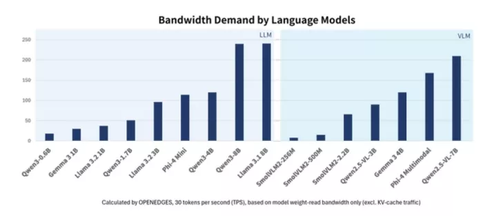
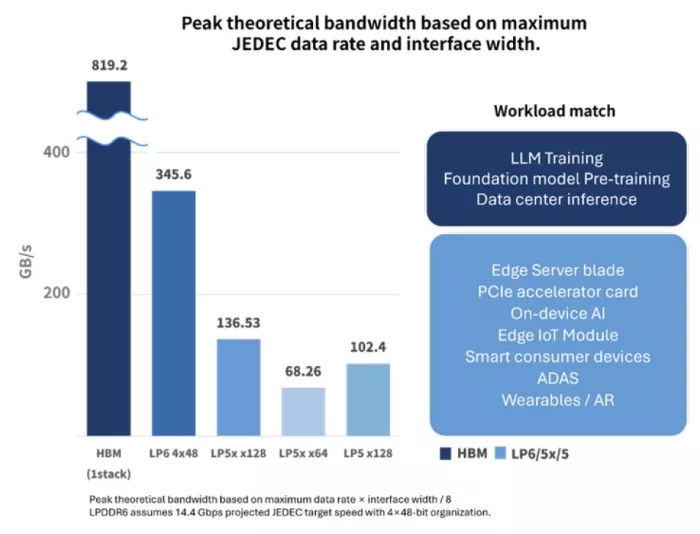
- Low power consumption: LPDDR5X delivers improved power efficiency compared to LPDDR5, helping reduce system power consumption in battery-powered AI platforms. [7]
- Cost efficiency: It provides a significantly lower unit cost compared to higher-bandwidth memory solutions, reducing total system cost.
- Supply stability: Samsung’s direct supply enables integrated procurement and supply chain simplification.
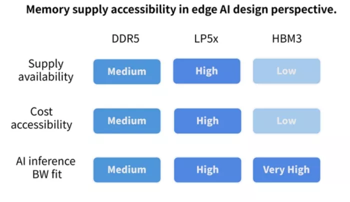
3. The Synergy: Why 8nm + LP5X Together
The power of this solution is not in either component alone, but in how the 8nm and LP5X memory can be co-optimized for the same class of workloads, enabling compact, efficient, and cost-sensitive AI inference.
When designed together as a system-level solution, the result is a total platform cost that is accessible to AI startups and fabless chip designers, along with a production-ready supply chain through Samsung Foundry that helps reduce vendor complexity.
Target Application: OPENEDGES’ Approach
OPENEDGES identified the combination of Samsung’s 8nm process and LPDDR5X (LP5X) memory as a highly practical foundation for AI GPU and inference accelerator development, particularly for AI platforms that must balance performance, power efficiency, and system cost simultaneously.
While the AI industry continues to push toward larger and more compute-intensive models, a rapidly growing portion of AI inference is expanding into distributed and edge-oriented deployment environments. These systems, ranging from industrial IoT devices and consumer electronics to compact AI accelerator modules and edge inference platforms, require commercially viable AI silicon solutions that can be deployed efficiently without the cost and complexity associated with leading-edge hyperscale AI infrastructure.
Within this landscape, OPENEDGES highlights 8nm + LP5X as a particularly well-balanced platform for scalable AI inference, offering sufficient memory bandwidth and compute capability while maintaining a practical balance of performance, power efficiency, and system cost.
The following sections highlight several application segments where OPENEDGES believes this combination delivers especially strong value and deployment practicality for next-generation AI inference platforms.
1. Edge AI/ IoT Devices
Industrial and commercial IoT applications increasingly require on-device AI inference, from smart cameras performing object detection, to environmental sensors running anomaly detection models, to industrial machines executing predictive maintenance algorithms. These devices share a common set of constraints:
- Tight power budgets (often battery or harvested energy)
- Limited thermal dissipation capability
- High production volumes requiring a competitive BOM cost
- Requirements for local inference without cloud dependency
2. On-Device AI (Smartphones & Consumer Devices)
The smartphone and consumer wearable market represent one of the largest volume opportunities for edge AI chips. Modern consumer AI features, including natural language processing, computational photography, real-time translation, and biometric authentication, all run as inference workloads directly on-device.
For fabless companies designing application processors or NPUs targeting this segment, 8nm + LP5X offers:
- A proven process node with established design flows for mobile SoC development
- LP5X memory interface compatible with existing mobile platform architectures
- Cost structure aligned with competitive smartphone BOM targets
- Power efficiency optimized for long-duration battery-powered operation
3. AI Accelerator Cards & Edge Inference Modules
A growing segment of AI startups is developing purpose-built inference accelerator modules, including PCIe cards, M.2 modules, and edge server blades, that plug into existing systems to add AI capability. For these products, 8nm + LP5X provides a well-matched platform for CNN and encoder-class AI inference workloads:
Compute density well-suited for INT8 and FP16 inference across a broad range of edge AI model architectures
LP5X memory bandwidth designed to support sustained batch inference without becoming a system bottleneck
A cost structure that scales with volume, supporting competitive module pricing as production ramps [8]
Why Samsung Foundry
Choosing a foundry partner is one of the most consequential decisions in chip development. Beyond process technology, startups and fabless companies need a partner capable of supporting them from first tape-out through volume production, with reliability, responsive support, and a stable supply chain.
Samsung Foundry’s 8nm process has already been proven in high-volume production across multiple customer programs, and this established track record provides practical advantages for new customers, including mature process design kits (PDKs) and yield models that enable more accurate cost projections at scale. Samsung Foundry also offers Multi-Project Wafer (MPW) options for first silicon and design validation, along with a commercial framework that can efficiently scale from prototype development to volume production.
Why OPENEDGES
OPENEDGES specializes in high-performance memory subsystem IP design suitable for many on-device AI chip development. Strategically, its business focuses on providing the most recent DRAM technologies in a more cost-efficient process node, like Samsung 8nm.
More specifically, OPENEDGES provides a one-stop total memory subsystem IP solution on the Samsung 8nm process, combining LP5X DDR PHY, memory controller and high-speed Network-on-Chip (NoC) IP to cover the entire memory subsystem design space in a SoC. This accommodates the complicated QoS requirements of an SoC that demands harmonized control of the entire memory subsystem, which is achievable by co-designing the memory subsystem IPs.
In addition, OPENEDGES offers an NPU IP solution supporting various CNN models and small language models (SLM), which is co-optimized with the total memory subsystem IP solution to take care of the huge memory bandwidth demand required for neural network inference workloads.

Get involved
AI startups, fabless design teams, and system integrators interested in evaluating the 8nm + LPDDR5X platform are welcome to reach out directly. We are actively engaging with design partners ahead of volume production and are open to early collaboration across the full design cycle.
Explore OPENEDGES IP:
Conclusion
The Edge AI market is large, fast-growing, and underserved by existing high-cost solutions. AI startups and fabless chip companies need a platform that delivers real inference performance within the power and cost constraints of edge products, not a scaled-down version of a data-center chip.
The Samsung 8nm + LP5X combination meets that need. It is a technically sound, commercially viable, and supply-chain-stable solution for the next generation of edge AI products. It is not the most expensive option, and it is not the cheapest. It is the right option for the workloads, customers, and markets where it is designed to compete.
Reference
[1] MarketsandMarkets, "Edge AI Hardware Market, Global Forecast to 2030," 2025. Available at: marketsandmarkets.com. The report projects the market to grow from $26.14B in 2025 to $58.90B by 2030 at a CAGR of 17.6%.
[2] MarketsandMarkets, 2025, ibid. Smartphones accounted for 80.5% of Edge AI hardware volume in 2024; inference workloads represented 99.8% of total market volume.
[3] Grand View Research, "Edge AI Market Size, Share & Trends Analysis Report," 2025. The manufacturing & industrial IoT segment is projected to grow at the fastest CAGR, driven by Industry 4.0 adoption including predictive maintenance, smart cameras, and factory automation.
[4] Grand View Research, 2025, ibid. Smart city and commercial display applications incorporate edge AI for real-time personalization, facial recognition, and adaptive content delivery across retail and public environments.
[5] Silicon Analysts, "Wafer Pricing by Process Node," April 2026. Available at: siliconanalysts.com/data/wafer-pricing. Actual contract pricing varies by volume commitment, customer relationship, and technology maturity. Figures are indicative only and do not represent Samsung Foundry's official pricing.
[6] LP5X is purpose-built for efficient AI inference at the edge, a use case defined by power efficiency, compact form factor, and cost-conscious design, rather than raw throughput at any price.
[7]JEDEC Solid State Technology Association, JESD209-5B: Low Power Double Data Rate 5/5X (LPDDR5/5X), July 2021. LPDDR5X is defined as an enhanced specification of LPDDR5, incorporating architectural improvements targeting higher data rates and reduced power consumption in mobile and embedded applications. Available at: jedec.org
[8] NRE, packaging, certification, and memory costs remain significant components of total BOM and should be evaluated on a per-program basis at target production volumes.
Related Semiconductor IP
Related Blogs
- How Cadence and TSMC Are Accelerating AI Silicon Design at Advanced Nodes
- Open-Silicon adds Silicon Logic Engineering - for a good reason
- Some critical considerations for SoC and Silicon Realization teams thinking about using ARM Cortex-A7 or ARM Cortex-A8 processor cores
- Experts Talk: RISC-V CEO Calista Redmond and Maven Silicon CEO Sivakumar P R on RISC-V Open Era of Computing