The $725 Million Chip Development: Why Execution Risk, Not IP Cost, Now Dictates Advanced-Node Survival

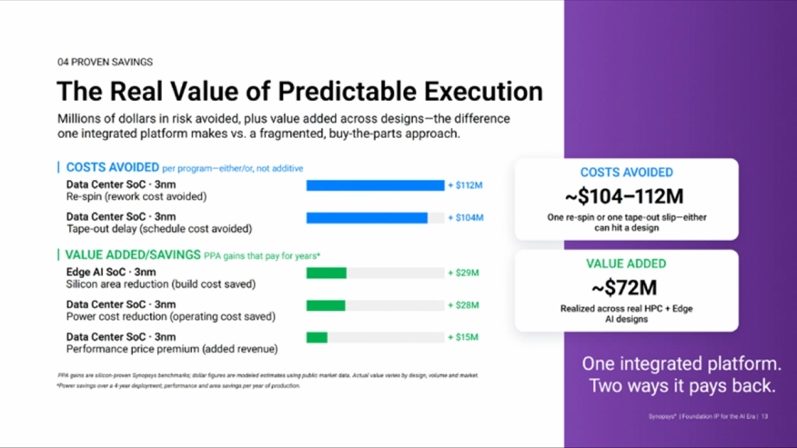 The philosophy of relying on a single, unified IP stack to lower your total cost of ownership is not a new concept invented just for the AI era. Semiconductor engineering teams have been weighing the trade-offs of piecemeal versus integrated intellectual property sourcing for decades. In previous process generations, veering away from a unified platform to cherry-pick individual components was often a tolerable compromise. The resulting vendor integration friction was an annoying operational tax, but it was rarely a fatal one.
In the AI era, however, that calculus has fundamentally shifted. As design costs surge toward three-quarters of a billion dollars at the 2nm node, and complex AI workloads push power delivery, operating voltage, and process variation to their absolute physical limits, the financial penalty for execution friction has been dramatically amplified. What was once a manageable integration headache has now become a multi-hundred-million-dollar program killer.
To read the full article, click here
Related Semiconductor IP
- UALinkSec Security Module
- Synopsys IO TSMC N3P GPIO 1.8V additional metal stack
- SLM SHS IP
- SLM High-Speed Access & Test IP
- PCIe 7.0 Controller (can be configured to support EP, RP, DM, or SW applications)
Related Blogs
- New Product Execution - It's Just not Good Enough
- Risk Avoidance, Hardware Emulation Style
- How to reduce the risk when making the shift to RISC-V
- Why Embedded MRAMs Are the Future for Advanced-Node SoCs
Latest Blogs
- The $725 Million Chip Development: Why Execution Risk, Not IP Cost, Now Dictates Advanced-Node Survival
- From photon to actuation: How physical AI is redefining embedded compute
- Secure Boot for embedded Linux on Efinix Ti375C529: Getting started with KiviBoot-Linux
- Akida in High-Frequency Trading: The Smart Signal Layer
- Cadence Expands Sovereign AI in Europe: From Chips to AI Factories