Beyond NVLink’s Rack: Meta and Panmnesia Bring CXL-Based Tight Coupling to the Whole Datacenter

- Meta and Panmnesia introduce a datacenter architecture that operates like a single chip — in an invited Review published by Nature Reviews Electrical Engineering (NREE).
- Built on the CXL standard, the design brings CPUs, accelerators and memory into one datacenter-scale coherence domain: up to approximately 13 times as many accelerators as NVIDIA’s rack-scale system (GB200 NVL72), with cross-rack access latency of several hundred nanoseconds — as much as an order of magnitude lower than the latency of conventional network-based infrastructure.
- Panmnesia has already implemented and validated the core components of the architecture in silicon.
Panmnesia, a fabless semiconductor company, and Meta, a global hyperscaler, have jointly proposed a next-generation artificial intelligence datacenter architecture in which an entire datacenter operates like a single chip. The work appears as an invited Review in Nature Reviews Electrical Engineering (NREE), a Nature Portfolio journal.

Figure 1. The CXL-based one-chip-like datacenter architecture introduced by Meta and Panmnesia in Nature Reviews Electrical Engineering, illustrating the idea of operating an entire datacenter as though it were a single chip.
The unit of AI execution is moving from one chip to the whole datacenter
As AI models grow into the trillions of parameters, a single training step can involve hundreds to thousands of accelerators exchanging terabytes of data. Because overall progress is set by the slowest participant, adding accelerators boosts compute capacity, but it also makes the system prone to frequent delays and failures caused by bottlenecking stragglers. When one component responds late, the rest stop and wait — and the wider the range of latency becomes, the harder it is to predict when a job will finish.
Narrowing that spread—and thereby creating a larger, more stable unit of execution—is an industry-wide challenge. Within a rack, devices are already tightly coupled through dedicated high-speed links. The next challenge lies in the segment beyond it — the connection between racks. Today, that segment still relies largely on general-purpose networks such as Ethernet or InfiniBand, where each request must pass through a network interface and a software-based coordination layer, each of which widens latency spread along the way. This work aims to bring greater predictability to this cross-rack segment.
Their foundation is Compute Express Link (CXL), an open industry standard. CXL is developed collaboratively by semiconductor and infrastructure companies, so it can be adopted across the industry without being locked into a single vendor's ecosystem. The architecture proposed by Panmnesia and Meta uses CXL to minimize latency variability beyond the rack. The goal is a datacenter that behaves with the predictability of a single chip.
At the core of the CXL-based architecture: three hardware elements and a hierarchical deployment
The proposed architecture places CPUs, accelerators and memory in a single CXL-based domain, extending the range over which cache coherence is maintained from within the rack to the datacenter as a whole. Three hardware elements — a high-fan-out non-blocking switch, a link acceleration unit (LAU) and a fabric controller — bound latency variability, and the resources themselves are laid out using the same principles that govern the placement of blocks inside a chip. To overcome the physical reach limits of electrical signaling, the Review also sets out how optical links (CXL-over-optics) can extend the reach of a CXL fabric. (Details are given in the Appendix.)
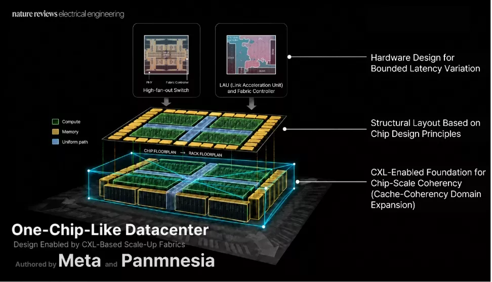
Figure 2. The one-chip-like datacenter concept: chip floorplanning principles carried over to a rack floorplan at datacenter scale. The design proceeds in three stages — (1) establishing the basis for chip-like operation with CXL, (2) adding dedicated hardware that bounds latency variability, and (3) arranging resources according to chip-architecting principles.
To gauge the effect of the architecture, the Review uses a conventional rack-scale configuration — one CPU coupled to two accelerators — as its reference point. Against that baseline, the number of accelerators a single CPU coordinates rises eightfold, from two to sixteen, and the coherence domain that operates as one unit grows to as many as 960 accelerators, roughly 13 times the reference platform. Accesses that once left the rack to traverse a network now follow a fixed path, with round-trip latency falling from the microsecond range to several hundred nanoseconds — as much as an order of magnitude lower. The unit of replacement after a failure also narrows from a whole server to a single device. Coupling devices at this scale into what behaves as one execution environment would make it possible to train a far larger single AI model without interruption, or to run multiple services concurrently on shared infrastructure without one stalling another.
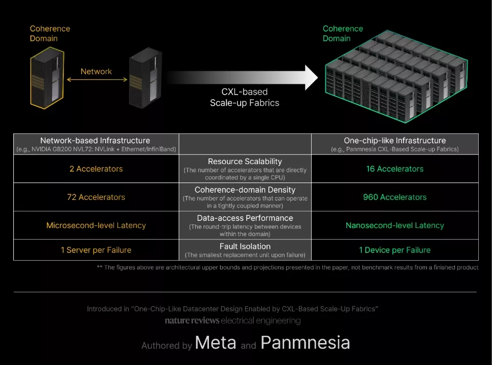
Figure 3. Architectural comparison between a conventional network-based infrastructure and a one-chip-like CXL fabric, contrasting coherence-domain size, cross-server access latency and fault-isolation granularity. The left-hand side uses NVIDIA’s GB200 NVL72 as the reference platform (NVLink and NVLink-C2C within the rack; Ethernet or InfiniBand between servers and racks); comparable technologies used for accelerator connectivity inside a rack, such as UALink, belong to the same category of rack-scale scale-up links. The right-hand side starts from the same baseline as the reference platform (two accelerators per CPU) and shows the configuration described in the Review, in which CXL.cache allows one CPU to coordinate 16 accelerators and roughly 60 such groups form a single coherence domain of up to about 960 accelerators. Note that the “72” at bottom left is the number of GPUs in a GB200 NVL72 rack (a product specification), whereas the “2 accelerators” at top right is the number of accelerators directly coordinated by one CPU as defined separately in the Review; the two figures rest on different bases.
Review articles in NREE are published by invitation only: the journal identifies a small number of researchers or organizations leading a given field and commissions the work from them. Nature’s selection of Panmnesia as an author on CXL-based datacenter architecture reflects recognition of the company’s technology as representative of the field. Panmnesia is the first semiconductor startup worldwide to lead an NREE Review, and the article is also the journal’s first Review to address CXL technology and AI datacenter architecture.
Myoungsoo Jung, CEO of Panmnesia, said, “As AI systems continue to scale, the ability to connect large numbers of accelerators and memory devices quickly and efficiently is becoming just as important as the performance of individual accelerators. This research outlines a direction for next-generation AI infrastructure, where CXL enables the entire datacenter to operate as a single computing system.”
Panmnesia has already implemented the architecture's core components in silicon, has completed validation, and is now preparing them for commercial supply. The Review is available at the link below.
Reference: Jung, M. et al. One-chip-like datacenter design enabled by CXL-based scale-up fabrics. Nature Reviews Electrical Engineering 3, 564–578 (2026).
https://www.nature.com/articles/s44287-026-00315-5
Appendix. Technical and Product Background
Background: the unit of AI execution has grown from a chip to a datacenter
As AI models have grown rapidly, so has the scale of hardware needed to run a single model — from an individual chip to something closer to a datacenter. NVIDIA has introduced the GB200 NVL72 rack-scale system, and AMD has unveiled its rack-scale AI system, Helios.
Two kinds of connectivity in today’s AI datacenters: scale-up and scale-out
Systems of this size are connected through two distinct layers.
Scale-up interconnects tie together devices in close physical proximity so that they behave like a single computer. NVIDIA’s NVLink and UALink, which is currently undergoing industry standardization, belong to this category. Because devices read and write one another’s memory directly, there is no need to package data for transmission and reception, which keeps latency low. NVLink and UALink are used mainly within a single rack today, and their focus on connecting accelerators to one another means they do not bring CPUs and memory into the same pool of resources.
Scale-out networks connect everything beyond that boundary. Racks and servers are linked over Ethernet or InfiniBand to grow the size of the system. This layer reaches much further, but data must be packaged into packets and pass through a software layer — and latency is correspondingly higher.
The problem today’s AI datacenters must solve
Large-scale AI training and inference proceed through repeated data exchange among the accelerators connected through these two layers. Since every accelerator must reach the same stage before the next stage can begin, the slowest among them determines the pace of the whole.
In current datacenters, accelerators inside a rack are joined by fast scale-up interconnects, while connections that leave the rack — and connections to devices other than accelerators — depend on slower scale-out networks. Measurements of such environments show heavy-tailed latency distributions, with 99th-percentile round-trip latency roughly five times the median. This is what holds the overall job back, and the more devices participate, the more often and more severely it occurs.
In large-scale AI infrastructure, reducing latency variation between devices so that the datacenter as a whole behaves predictably matters as much as improving individual-device performance or link speed.
Panmnesia and Meta’s proposal: a one-chip-like AI datacenter architecture
To address the problem, the Panmnesia and Meta research team looked at how it has already been solved inside a semiconductor chip. Within a chip, CPU cores, accelerators and memory are joined by short and uniform paths, so signals arrive in consistent time; they share one memory space, and hardware automatically keeps the data each component sees up to date. Extending that predictability across servers and racks to the whole datacenter is the starting point of this work.
The one-chip-like datacenter architecture the team proposes has three stages.
1. Establishing the CXL foundation
The team identified cache coherence — the mechanism by which multiple components share a single memory space and are automatically kept in step with the latest data — as the key function behind a chip’s predictable behavior. To extend that function across many servers, they built on CXL, which supports it as part of the standard.
CXL is itself a scale-up interconnect. Unlike existing scale-up interconnects, which focus on linking accelerators to one another, CXL brings memory into the same connection alongside CPUs and accelerators and maintains cache coherence among them at the level of the standard. It also supports a wider range and number of devices. That is why the team chose it: to extend the scale-up domain, until now used mainly within a single rack, out to datacenter scale.
The CXL standard, however, defines only the basic rules for joining devices together; how data is routed and the resulting latency are left to the implementer. Following the standard alone therefore leaves the time spent at each device uneven. Closing that gap is what the team treats as the core contribution of this work.
2. Three dedicated hardware elements that reduce and bound latency variation
On top of CXL, the team adds three hardware elements:
- High-fan-out non-blocking switch: connects many devices at once, reducing the number of hops and keeping path lengths similar regardless of the source.
- Link acceleration unit (LAU): moves repetitive protocol processing at each connection point onto a dedicated hardware pipeline, making hop-level behavior more regular and bounding latency variation.
- Fabric controller: applies the same ordering policy for handling requests across the entire system, so that transactions are processed consistently no matter which device they pass through.
3. Deployment that follows chip-architecting principles
Finally, these components are arranged on the same principles as a chip. Just as a chip groups functional blocks into tiles, the architecture groups CPUs, accelerators, memory, and switches by function into trays, groups trays into pods, and connects pods through a fabric — a regular tray–pod–fabric hierarchy designed to preserve fixed-hop, more consistent communication paths and timing.
Quantified improvements
With consistent paths, consistent processing time and a consistent ordering policy working together, devices spread across multiple racks begin to behave as one execution environment. The Review presents the following improvements relative to conventional scale-out network-based infrastructure. The basis for comparison is NVIDIA’s GB200 NVL72, in which one CPU is coupled to two accelerators over NVLink-C2C, the rack interior is connected by NVLink, and servers and racks are joined by a scale-out network such as Ethernet or InfiniBand.
- Accelerators directly coordinated by a single CPU: 2 → 16 (an eightfold increase)
- Accelerators operating together in one coherence domain: tens → up to approximately 960
- Data-access latency between devices: microsecond-level → several hundred nanoseconds (roughly an order of magnitude lower)
- Replacement unit on failure: an entire server → a malfunctioning single device
Separating resources by type allows the system to replace only the malfunctioning devices rather than an entire server, avoiding wasted resources and prolonged operational halts.
Beyond a concept: silicon implementation and productization
The design is not merely conceptual. Panmnesia has implemented the components described above in silicon and is preparing them for productization. The fabric controller (a combined CXL/PCIe controller) and the LAU have completed silicon validation, and the fabric switch has been fabricated as a physical silicon chip, with pre-release silicon now being supplied. This demonstrates that the proposed architecture holds at the level of manufacturable silicon.
The floorplans of Panmnesia’s CXL switch and fabric controller chips, included in the Review, bear this out. Global control logic sits at the center of the die, and the ports that connect to external devices are placed symmetrically around its periphery. This gives every connected device the same signal travel distance, eliminating the probability of the arrival time difference that would otherwise stem from the port's physical location. Each port integrates the link acceleration unit, the fabric controller and local buffering into a single block, so that data entering through any port is processed in the same order. In other words, the design principles above are realized in the physical layout of an actual chip rather than remaining a concept.
Security and remaining challenges
Where several AI workloads run at once, there is a risk that data belonging to different tenants could be unintentionally shared or exposed. To prevent this, the Review covers clearly bounded isolation domains for each tenant, hardware-enforced access control that allows access only to authorized tenants, and encryption of data in transit. These mechanisms address key security requirements for production deployment.
Another challenge is that electrical signals have the physical limitation of weakening over long distances. At the latest signalling rate (128 GT/s), even with two retimers in series, the reach over which a signal arrives reliably is roughly seven meters — about six to seven racks. To push past this and extend the scale-up domain across a whole datacenter, the team proposes keeping the rest of the design intact and carrying the signal optically rather than electrically (CXL-over-optics). Panmnesia has also built this approach in hardware and completed proof-of-concept validation.
As the unit that runs an AI workload grows from an individual server to an entire datacenter, the significance of this work lies in setting out design principles for connecting systems not merely at greater scale but with the predictability of a chip — and in implementing and validating them in real silicon. By structurally reducing latency variation between devices, the approach is expected to provide a foundation for improving both the performance and stability of large-scale AI infrastructure.
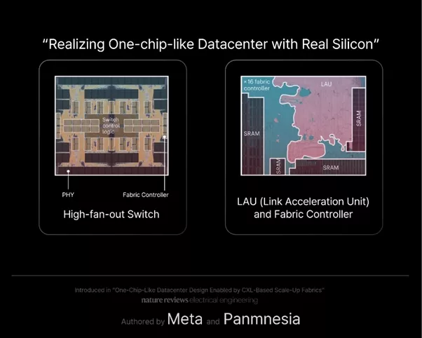
Figure 4. Key components that minimize latency variability — high-fan-out switches, link acceleration units (LAUs), and fabric controllers.
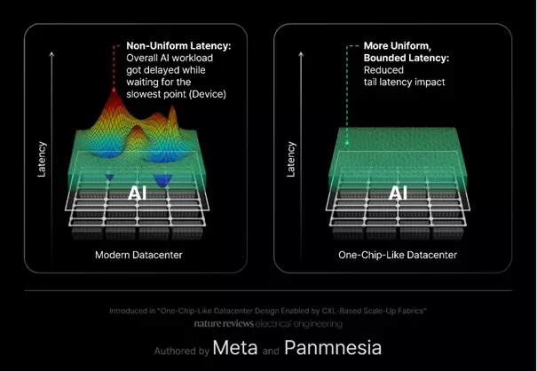
Figure 5. Comparison of device-to-device latency distributions. In a conventional datacenter (left), latency spikes sharply at certain points (non-uniform), forcing the entire job to wait on the slowest link. In a one-chip-like datacenter (right), the architecture aims to make latency more uniform and bounded across the fabric, reducing the impact of tail latency.
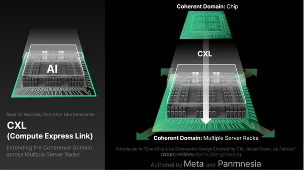
Figure 6. CXL as the foundation of the one-chip-like datacenter. CXL extends shared address-space access and hardware-managed coherence beyond the CPU package and across disaggregated devices, providing the foundation for multi-server one-chip-like organization.
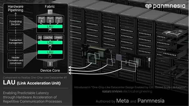
Figure 7. Component ①: Link acceleration unit (LAU). Repetitive processing at device-to-device connection points — forwarding decisions, transaction management, and header translation — is handled by dedicated hardware, so that communication always completes within a bounded time.
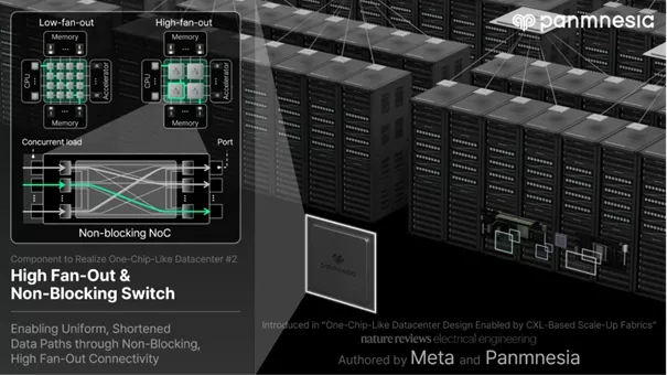
Figure 8. Component ②: High-fan-out non-blocking switch. It connects many devices in few hops and provides ample internal paths, so that path lengths remain comparable regardless of the source device and concurrent requests do not block one another.
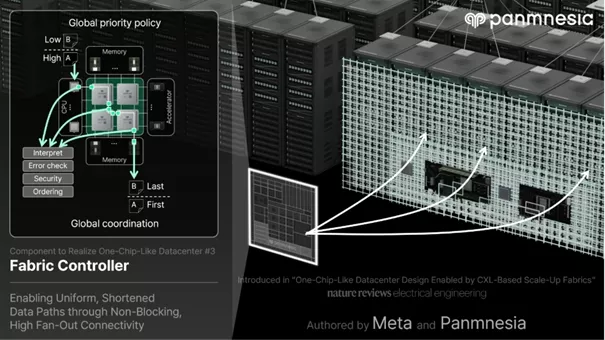
Figure 9. Component ③: Fabric controller. It applies a single set of rules for request handling — priority, interpretation, error checking, security, and ordering — uniformly across the system, so that requests are processed consistently no matter which device they traverse.
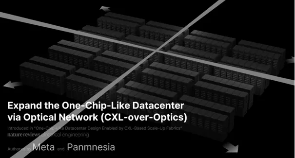
Figure 10. Scaling through CXL-over-Optics. By carrying signals optically while leaving the higher-level design unchanged, the approach moves past the reach limit of electrical signaling (roughly 7 m, or six to seven racks) and extends the one-chip-like datacenter across the entire facility.

Figure 11. Myoungsoo Jung, CEO of Panmnesia
Explore Panmnesia IP:
Related Semiconductor IP
- Link Acceleration Unit
- Link Controller IP
- CXL - Enables robust testing of CXL-based systems for performance and reliability
- CXL Verification IP
- CXL 4 Verification IP
Related Blogs
- ARM's Cortex-A15: A big step up for the ARM processor architecture. Targeting 32nm and 28nm technology nodes
- Arteris vs Sonics battle...Let's talk NoC architecture
- ARM V8 Architecture
- PCIe Ready for Datacenter Role
Latest Blogs
- From Bug Hunting to Engineering Methodology: Lessons from AI-Driven Development
- Manufacturing Intelligence: Turning EDA Data into Trusted Action
- Execute-in-Place: Getting More from Embedded NVM
- Rethinking RTL flows with AI-driven hybrid formal verification
- Arm and NVIDIA: Building the trusted compute foundation for the agentic AI era