Cadence Achieves Successful Silicon Validation of 1st IP Test Chips on Intel 18A
Cadence has reached an important milestone in its collaboration with Intel Foundry with the successful completion of its first test chips on Intel 18A earlier this year. This achievement marks a meaningful step forward in enabling advanced, standards‑based interface IP on Intel 18A. More details about these test chips were recently shared in presentations at CadenceLIVE Silicon Valley and GOMACTech events.
As system architectures continue to evolve to support AI, high‑performance computing, and heterogeneous designs, early validation on silicon plays a vital role. This set of first test chips on Intel 18A reflects Cadence's continued investment in silicon‑backed IP readiness, providing customers with practical insight and reduced risk as they make IP decisions.
Advancing From Early Enablement to Silicon Validation on Intel 18A
The completion of these test chips represents a transition from early enablement activities into tangible silicon validation, using dedicated vehicles to exercise real interface behavior under representative operating conditions. The silicon-validated IP serves as a proof point for the GAA (RibbonFET) and back-side power (PowerVia) technology available on Intel 18A.
Yet rather than serving as a single proof point, each test chip supports ongoing learning across electrical performance, signal integrity, power behavior, and system integration assumptions. These insights feed directly back into model correlation and IP refinement, strengthening readiness well before customer designs move toward production.
This approach reflects a simple but critical principle: early silicon matters. It shortens learning cycles, uncovers integration considerations sooner, and helps ensure that IP entering customer SoCs is aligned with real‑world behavior on advanced nodes.
Key IP Enabled on Intel 18A
The test chips on Intel 18A technology bring together several cornerstone interface technologies from Cadence's IP portfolio, each aligned with the bandwidth, latency, and integration demands of modern systems.
High‑speed 112G PAM4 SerDes IP was exercised on Intel 18A as a foundation for bandwidth‑intensive AI, networking, and accelerator applications.
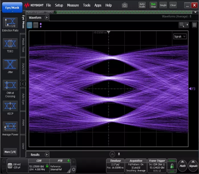
Figure 1: 112G SerDes PAM4 eye diagram
The test chips also support PCI Express® (PCIe®) 6.0 (64 GT/s PAM4) and PCIe 5.0 (32 GT/s NRZ) PHY IP operation, reflecting the continued evolution of high‑bandwidth I/O and coherent system architectures.
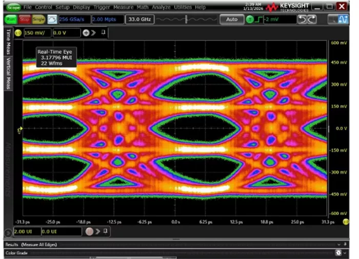
Figure 2: PCIe 6.0 Eye Plot
For the memory subsystem, LPDDR5 PHY IP was validated at high data rates on Intel 18A, supporting the power‑efficient, high‑performance memory interfaces required for advanced SoCs.
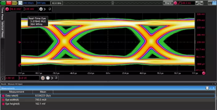
Figure 3: LPDDR5 8533 Mbps Tx/Rx Eye Diagram
Also demonstrated in the test chips was UCIe™ IP, including multi‑lane configurations and packaged implementations that align with emerging chiplet‑based system designs.
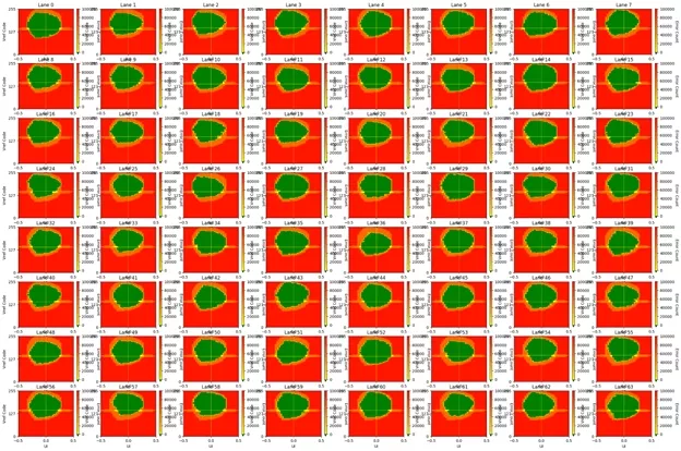
Figure 4: UCIe-AP 16G Eye Plot – 64 Lanes
Together, these protocols represent the interfaces that increasingly define system scalability—not in isolation, but in combination. Validating them on silicon helps ensure they operate cohesively across SoCs, packages, and multi‑die systems.
Reducing Risk for Advanced Designs
Early test chips play a critical role in helping customers move confidently onto new process technologies. With these test chips, Cadence can validate key interface behavior on real silicon, strengthen correlation between design models and measured results, and identify integration considerations at a stage when design flexibility is still high.
This silicon work complements Cadence's broader collaboration with Intel Foundry, including Design IP expansion, EDA tool enablement, and advanced packaging support. Taken together, these efforts are focused on a shared goal: accelerating time‑to‑value while reducing uncertainty for customers building next‑generation systems.
Continuing Momentum with Intel Foundry
Cadence remains focused on delivering IP that is not only standards‑based but backed by real silicon validation. The completion of the first test chips on Intel 18A represents an important milestone—one that reinforces Cadence's long‑term commitment to enabling customers with reliable, production‑ready IP as they move onto Intel Foundry technologies. Meanwhile, Cadence is continuing its collaboration with Intel Foundry on Intel 18A-P and Intel 14A technology nodes.
Learn more about Cadence Design IP.
Related Semiconductor IP
- 112G-ULR PAM4 SerDes PHY
- SerDes IP
- DSP-Based 112G SerDes
- 112G Ethernet PHY in TSMC (N7, N5, N3P)
- 112G-VSR PAM4 SerDes PHY
Related Blogs
- T&VS provides solution to Post Silicon Validation
- From "What-If" to "What-Is": Cadence IP Validation for Silicon Platform Success
- Intel -- The Litmus Test
- T&VS delivers Emulation and Validation services for Mobile SoC
Latest Blogs
- World's First Standards-Compliant 112G PHY IP for Linear Optics: A Turning Point for AI Interconnects
- One Key for Every Door: How Aliro Extends the UWB Digital Key Beyond the Car
- Reprogrammable Post-Quantum Security for SoCs: Why Crypto-Agility Matters
- Designing the Beam Steering Core for a C-Band AESA: A Look at VSI's VBF0644 GaAs Beamformer IC
- Secure Boot for embedded systems: Building a complete chain of trust